
| ||||||||||||||||||||
 |
|
VLSI GROUP A:
Horwitz, Seth Allen | ||||||||||||||||||
| ||||||||||||||||||||
VLSI DESIGN
|


 |
|||||||||||||||||||

Date: 16 September 1997
Design Purpose:
|
To design a 16 bit floating point addition/subtraction & shift register unit.
|
||||||||
Input Pin Allocation:
|
8 Pins
Datapath
1 Pin
Reset
2 Pins
Control Input A/B & Hi/Low
4 Pins
Operation Code
An 8 bit bus will receive the two 16 bit floating point inputs using the Hi/Low halves with 2 clock
cycles each. A reset signal can be used to return to unit to the initial state and should remain de-
asserted during normal operation. The Operation Code allows the user to choose the various func
tions of the unit which includes: addition, subtraction, shift left, shift right, and other undeter
mined functions. | ||||||||
Output Pin Allocation:
|
8 Pins
Datapath
2 Pin
Error Bits (Underflow/Overflow)
4 Pins
States Output
4 Pins
Register Output
An 8 bit bus will be used as the output for the results of all functions in the unit. Error bits are
included to indicate overflow, underflow, and any other general error signal. | ||||||||
Remarks:
|
Our functional description will be more detailed as the project progresses. As for most projects, we foresee our primary constraint/concern would be that of the space limitations set forth by the project specifications. Depending on the amount of space we have available, we may include other floating point operations in the unit. |
Date: 15 December 1997
Project Title:
|
Sandman a.k.a. FP4MENU |
||||||||||||||||||||||||||||||||||||||||||
Functional Purpose:
|
To design a 16 bit floating point addition/subtraction unit that outputs a normalized result and accounts for overflow, underflow, and many common cases.
|
||||||||||||||||||||||||||||||||||||||||||
Input Pin Allocation:
|
Pin 0
Floating point input A3 & A11
Pin 1
Floating point input A2 & A10
Pin 2
Floating point input A1 & A9
Pin 3
Floating point input A0 & A8
Pin 4
Operation Code 1
Pin 5
Operation Code 0
Pin 6
RESTART
Pin 8
Floating point input A4 & A12
Pin 9
Floating point input A5 & A13
Pin 10
Floating point input A6 & A14
Pin 11
Floating point input A7 & A15
Pin 12
CLOCK A
Pin 13
Floating point input B7 & B15
Pin 14
Floating point input B6 & B14
Pin 15
Floating point input B5 & B13
Pin 16
Floating point input B4 & B12
Pin 21
CLOCK B
Pin 26
Floating point input B3 & B11
Pin 27
Floating point input B2 & B10
Pin 28
Floating point input B1 & B9
Pin 29
Floating point input B0 & B8
An 8 bit bus will receive the two 16 bit floating point inputs using the Hi/Low halves with 2 clock
cycles each. A RESTART signal can be used to return to unit to the initial state and should remain de-
asserted during normal operation. The Operation Code allows the user to
choose between the functions addition and subtraction. | ||||||||||||||||||||||||||||||||||||||||||
Output Pin Allocation:
|
Pin 19
UNDERFLOW indicator
Pin 20
OVERFLOW indicator
Pin 22
Floating point output OUT0 & OUT8
Pin 23
Floating point output OUT1 & OUT9
Pin 24
Floating point output OUT2 & OUT10
Pin 25
Floating point output OUT3 & OUT11
Pin 30
Floating point output OUT7 & OUT15
Pin 31
Floating point output OUT6 & OUT14
Pin 32
Floating point output OUT5 & OUT13
Pin 33
Floating point output OUT4 & OUT12 An 8 bit bus will be used as the output for the results of all functions in the unit. Error bits are included to indicate overflow, underflow, and any other general error signal. | ||||||||||||||||||||||||||||||||||||||||||
MiscellaneousPin Allocation:
|
Pin 7
Reserved
Pin 17
Reserved
Pin 18
Reserved
| ||||||||||||||||||||||||||||||||||||||||||
Remarks:
|
The original design allowed for enough leeway for the construction of a floating point multiplier to complement the addition function. However partly due to a flawed assumption that all members of the team would at least attempt to contribute, the main part of the project - that being the addition function - was left in disarray as the multiplication function was completed. Comparing the trade off between a fully functioning multiplier coupled with an addition function that accounted for most of the reasonable cases and working completely on the addition function to have it encompass as much as possible, what remained of the team decided to go for the latter. The multiplication unit is appended at the end of this project for your entertainment value. |
Date: 15 December 1997
Distribution
| Horwitz, Seth Allen
| Walker, Raymond "Floyd"
| Wu, Dennis
|
|
|||
Machester Adder Unit & Testing: |
. | . | . |
Latch Units & Testing: |
. | . | . |
Register Units & Testing: |
. | . | . |
Barrel Shifter & Testing: |
. | . | . |
Multiplexer/Selector Units & Testing: |
. | . | . |
Decoder Unit & Testing: |
. | . | . |
Shift Register Units & Testing: |
. | . | . |
Priority Encoder Unit & Testing: |
. | . | . |
|
|||
Addition Unit & Testing: |
. | . | . |
Multiplication Unit & Testing: |
. | . | . |
Addition Normalization Unit & Testing: |
. | . | . |
Multiplication Normalization Unit & Testing: |
. | . | . |
Programmable Logic Array Unit & Testing: |
. | . | . |
|
|||
Overall Layout of Project: |
. | . | . |
Overall Testing of Project: |
. | . | . |
Spice Simulation of Project: |
. | . | . |
Crystal Analysis of Project: |
. | . | . |
Presentation of Project: |
. | . | . |
Project Report: |
. | . | . |
Project Web Page: |
. | . | . |
|
|||
Comments pending a discussion with Dr. Cavallaro. | |||
Date: 15 December 1997
................
|
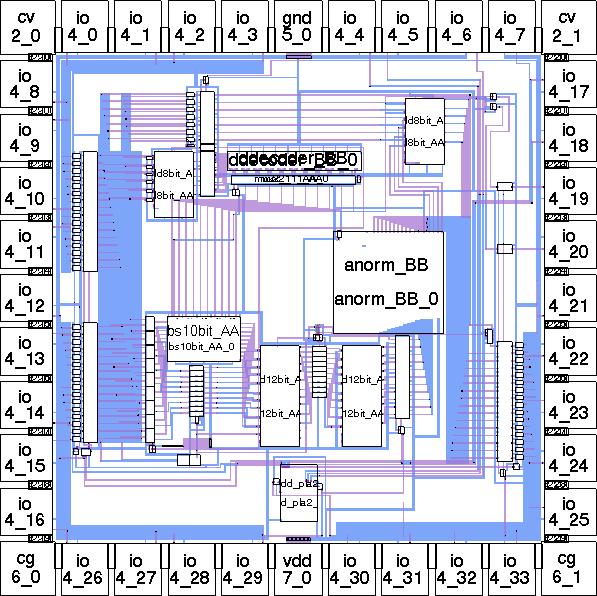
The following is the overall schematic of Sandman (a.k.a. FP4MENU). All
components in the following schematic is expandable (even the filler blocks
and I/O pads). Please feel free to click on ANY component to further
explore the details of the design, the irsimulation results, the spice
results, as well as the crystal analysis results. [FEEL FREE TO EXPAND
THE UNITS MORE]
|
Date: 15 December 1997
Date: 15 December 1997
................
|
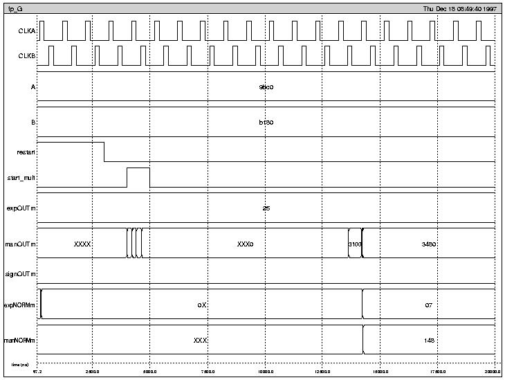
The original designed schematic of Sandman (a.k.a. FP4MENU) included a
compact multiplier structure, which was tactically removed in order to
relinquish space for the bulkier floating point addition function. This
multiplier is fully functioning and awaits a chip area increase.
NOTE : The resulting values from the multiplication can be plugged through
the same normalization unit as the addition function to yield the desired answer.
|
|
| |
Date: 15 December 1997
Date: 28 April 1997
Date: 28 April 1998
Request : |
Report |
ID : |
53613 |
P-Name : |
Sandman |
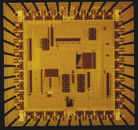
Fab-ID : |
N81X BL |
P-Password : |
. |
Report : |
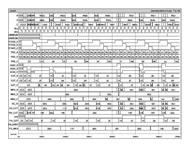
This is a floating-point addition chip, which adds two 16-bit numbers
together. The exponnent is 6 bit represented as bias 31. The mantissa
is represented as sign magnitude. 9 bits for the magnitude and 1 bit
for the sign. The chip reports underflow and overflow. NaN, Inf, -Inf,
and un-normalized numbers are not implemented.
All of the chips were only partially functional. However, they all produced
identical output, which leads me to believe that it was a design flaw. The
errors appear to involve the normalization. The error appeared to be in-
correct pre-normalization causing all further output to be flawed.
Our first test used various combinations of positive and negative numbers
of differing exponents. The second test would test the functionality of the
underflow and overflow bits, but since the earlier test failed we did not
move onto other tests.
Although, the test did not work as predicted on any of the chips, the output
becomes inconsistent at speeds of 17Mhz and greater. We predicted a speed
of 10Mhz, so in that regard it functioned as predicted. It is important
to note that we tested at 6.8Mhz and then 17Mhz, so the actual failure point
is not known.
|
Report URL : |
http://www.ece.rice.edu/Courses/422/1997/chewy/vlsiindex.html |
Submitted By : |
Raymond "Floyd" Walker (blindman@owlnet.rice.edu) |
Request : |
END |

Last modified: Wed Apr 29 03:36:21 CDT 1998