Previous Tutorial
Main Menu
Next Tutorial
Using the Virtuoso Layout Editor
We are now going to build the mask layout view of our cmos inverter.
Since we intend
to use these standard cells with the automatic place and route, it is
important to remember that vias must be at the intersections of the routing grid.
If you have not already, please familiarize yourself with the routing grid here. For your first layout we will give you the coordinates of the design, but for future standard cells it might be helpful to build a the routing grid using text rectangles to guide the layout process.
To create a cell named "inv" in your new library,
First select File -> New -> Cellview ... from either the library manager or CIW windows.
A Create New File form pops up.
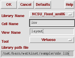
Enter the name of your local library as Library Name; enter "inv" as Cell Name, "layout" as View Name; select "Virtuoso"
for Tool then click "OK".
Cell "inv" with "layout" view will be opened in your library for you to edit.
Two more windows will be brought up. The first one is
Layer Select Window (LSW).
The second one is Virtuoso Editing window.
LSW
LSW displays the layers defined in the technology. Not all of the layers are currently visible.
To select which layers you want to view, go to Edit -> Set Valid Layers ... The layers with the highlighted boxes next to them will appear in your LSW window.
Another useful feature of the LSW are the AV NV AS NS buttons. These buttons speficy which layers in the layout window can be viewed or selected.
- AV all viewable
makes all layers visible
use redraw or CTRL-r for this to take affect
- NV none viewable
make all layers except the one currently selected in the LSW invisible
select other layers in LSW to make them visible as well
Middle-clicking a layer in the LSW toggles view on and off
use redraw or CTRL-r for this to take affect
- AS all selectable
allows you to select any layer
Pin layers and instance (subcells) selection controlled by Inst and Pin at top of window
- NS none selectable
Turns off selection of layers (darkens layer in LSW window)
Right-clicking a layer in the LSW toggles select on and off
Try playing with these features after you have drawn some rectangles in the next section.
You might notice that some layer names appear more than once. For example metal1 appears twice: once as metal1 dg, the again as metal1 pn.
"metal1 dg" is metal1 layer with drawing purpose. Layers with drawing
purpose will show in the mask layout. "metal1 pn" is metal1 layer
with pin purpose. Layers with pin purpose are not part of the mask layout.
They indicate position of I/O pins for automatic routers.
Virtuoso Editing Window
Useful commands
Window -> Zoom has a few options for zooming, but you may find the
following shortcuts useful.
To zoom out, type shift-z, to zoom in type control-z or click
and drag with your right mouse button to zoom to the area under the rectangle
created by dragging. Be careful with the last option, a single right click
repeats the last command).
Use the bind key k to bring up the ruler command. left click on two points to draw a ruler on the design (measures in microns). This is a handy
in determining whether or not you are following the spacing rules.
Drawing a rectangle
The most common shape in a layout is rectangle. To draw rectangles
-
From LSW select a layer by clicking left mouse button on
it. You will see the selected layer surrounded by wider border (the selected
layer is hightlighted).
-
From Virtuoso Editing window pull down menu, select
Create
-> Rectangle r
Comment: Create Rectangle has bind key "r", and it is listed
in graphic tool bar too.
-
In the layout design window (Virtuoso Editing) click left
mouse button for the first corner of the rectangle, then click left mouse
button again for the second corner. A rectangle is drawn.
-
If this is not the desired rectangle, select Edit -> Undo u
from menu to undo the action. Do you know the bind key for undo? The key
right after the command is the bind key.
-
If you want to draw another rectangle using current drawing layer, simply
click left mouse button for the two corners of the rectangle.
-
If you want to draw rectangles of another layer, click left mouse button
to select your layer in LSW to change the drawing layer then
click left mouse button for the two corners in Virtuoso Editing
window.
-
If you have finished drawing rectangles, hit < Esc > on the key
board to exit the "Create Rectangle" command.
Drawing a polygon
Another useful shape is the polygon. To draw a polygon
- From the Virtuoso Editing window pull down menu, select Create -> Polygon P or use the P bind key.
- In the layout design window click the left mouse button for the first point of the polygon.
- Continue clicking to place other corners of the polygon.
A dashed line will show you the rest of the current shape. Double-click and cadence will fill out the rest of the shape according to the dashed line.
- You can also complete the polygon by clicking on the initial point.
If you have finished drawing polyons, hit < Esc > on the key
board to exit the "Create Polygon" command.
Drawing a path
Paths are easy ways to route metal layers. To create a path
- From the Virtuoso Editing window pull down menu, select Create ->Path p or use the p bind key.
- The Path Menu will pop up. Try selecting different metal layers from the LSW. Notice that the width field in the Path Menu is different for metal3 and metal1. The width default is the minimum routing width, you can choose to increase it, but anything less will cause design rule errors.
- Now look at the Change to Layer box in the Path Menu This lists the layers available from the current layer selected in the LSW. If metal1 is selected in the LSW and metal2 is selected in the Change to Layer window, the first time you click on the Virtuoso Layout Editing window, a m2_m1 via will appear. This is a quick way to change between layers.
- Try drawing some paths and changing layers until you get the hang of it. Double-click to end a path.
- If you ever need to change a path, there are a few ways to do it.
One is to select the path in the editing window and use the bind key q to bring up the Edit Path Properties box. By changing the coordinates in the Points box the location of sections of the Path can be modified. A simpler method for editing paths is to type F4 to change the (F)Select: at the top of the Layout Editing window to (P)Select:. Now you can select and drag individual sections of the path and not have to worry about exact coordinates (this also works with rectangles and other shapes).
Change snap to 0.15
If you are using the 0.5 micron technology, make sure that lambda is 0.15
(actually, lambda is .3 microns, but the routing resolution is 1/2 lambda).
To do so follow the following proceedure once you have opened a layout window.
In the layout window, click on Options -> Display
A Display options window pops up.
Change the "X snap spacing" &
"Y snap spacing" to 0.15.
Click on OK.
Start building the Inverter
Finally we are going to build
a PMOS transistor and a NMOS transistor by drawing rectangles, polygons, and paths in various
layers. Notice that we are using scalable Nwell submicron technology and
the layers below are layers with drawing purpose. The numbers refer to the coordinates of your mouse (X,Y), displayed in the upper left-hand portion of the screen. Please draw every shape with care.
Rectangles
| Layer |
first corner |
second corner |
| pselect dg |
(0.00, 10.50) |
(4.80, 16.80) |
| nselect dg |
(0.00, 1.20) |
(4.80, 5.40) |
| active dg |
(0.60, 11.10) |
(4.20, 16.20) |
| active dg |
(0.60, 1.80) |
(4.20, 3.90) |
| nwell dg |
(-2.40, 7.20) |
(7.80, 19.80) |
Polygon
| Layer |
first point |
second point |
third point |
fourth point |
fifth point |
sixth point |
seventh point |
eighth point |
| poly dg |
(2.10, 1.50) |
(2.70, 1.50) |
(2.70, 16.80) |
(2.10, 16.80) |
(2.10, 6.90) |
(0.60, 6.90) |
(0.60, 5.70) |
(2.10, 5.70) |
Save you Design:
It is good practice to save your design every few minutes to prevent loss
of your design in case cadence crashes on you.
To save your design
Click on Design -> Save.
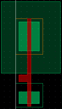
Now you have drawn the diffusions and a poly contact for gate. You are
ready to put down the metal contact for the sources and drains. For this
we will use pre-defined contacts. In the Layout Editing Window type i
for the instance bind key (or Create -> Instance in the pull-down menus)
Now browse to find cell m1_n in the library you created. This
contact is simply a 0.6u square of layer cc surrounded by two 1.2u squares
of metal1 and active, enclosed by a 2.4 square of nselect. Left-click at
(0.9, 2.1) to place the first instance and (3.3, 2.4) to place the second. To expand the view of the instance, type Shift-F (Control - f toggles back to unexpanded view).
Now change from m1_n to m1_p to place the source contacts. The
Only difference between the m1_n and m1_p contacts is that nselect is replaced
with pselect. The m1_p contacts should be placed at (0.9, 12.3), (0.9, 13.8),
(0.9, 15.3), (3.3, 12.3), (3.3, 13.8), and (3.3, 15.3).
Now to add a few metal1 connections.
Rectangles
| layer |
first corner |
second corner |
| metal1 dg |
(0.60, 13.20) |
(1.80, 17.10) |
| metal1 dg |
(3.00, 11.70) |
(4.20, 15.90) |
| metal1 dg |
(0.60, 0.90) |
(1.80, 3.00) |
Paths
| layer |
first point |
last point |
| metal1 dg |
(3.60, 2.10) |
(3.60, 15.90) |
| metal1 dg |
(1.20, 12.00) |
(1.20, 14.10) |
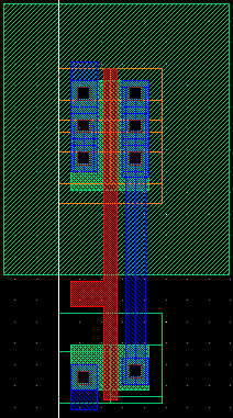
The contacts on the drain of PMOS are now connected to the contacts on the
drain of the NMOS. To make this inverter work, we need power supplies. The ntap
and ptap instances provide substrate contacts for the design.
Rectangles
| layer |
first corner |
second corner |
| metal1 dg |
(-0.60,17.10) |
(5.40,18.90) |
| metal1 dg |
(-0.60,-0.90) |
(5.40, 0.90) |
Contacts
| Instance |
first contact |
second contact |
| ptap |
(-0.30, -0.30) |
(4.50, -0.30) |
| ntap |
(-0.30, 17.70) |
(4.50, 17.70) |
Okay, we can now draw the input and output pins. Begin by placing an
m1_poly instance (poly to metal1 contact, uses poly instead of active
and no select rectangle) at (0.90, 6.00), a metal1 dg rectangle at (0.6, 5.1),
(1.8, 5.7), and a metal1 dg path from (1.2, 4.5) to (1.2, 7.5).
It looks like the inverter layout has been finished. But in order to
let the router know how to connect this cell to others, pins are needed
for inputs, outputs, and power supply nodes. Pins define where the wires
outside the cell can be connected to the cell. The input pin will be a,
the output pin will be y, power is called vdd! and ground gnd!.
Before placing the pin, it is a good idea to get into the habit of placing
metal rectangles in the appropriate layer. This becomes more important in
hierarchical designs when the metal over which the pin is being created might only exist in a subcell, and not on the current level.
Rectangles
| layer |
first corner |
second corner |
| metal1 dg |
(0.75, 4.05) |
(1.65, 4.95) |
| metal1 dg |
(0.75, 7.05) |
(1.65, 7.95) |
| metal1 dg |
(3.15, 4.05) |
(4.05, 4.95) |
| metal1 dg |
(3.15, 7.05) |
(4.05, 7.95) |
| metal1 dg |
(3.15,10.05) |
(4.05,10.95) |
To create all of these pins
-
From Virtuoso pulldown menu, select Create ->
Pin...
.
This brings out a Create Symbolic Pin form. Select "shape
pin" in Mode field, then a Create Shape Pin form comes
out.
Comment: You might get Create Shape Pin form in the first
place.
Comment: Bind key for Create Pin is "^p" which means
"Control-p".
- By Mode select "rectangle" and select "Display Pin Name
"
-
Enter "a a y y y vdd! vdd! gnd! gnd!" as Terminal Names.
When you enter more than one terminal names,
Layout Editor will create these pins sequentially. We are creating
multiple copies of each pin to allow more efficient autorouting.
Comment: "vdd!" and "gnd!" are names reserved for power
pins. Don't use these names for other purposes.
-
The first pin to create is "a". In LSW,
select metal1 pn pin layer (the metal1 layer with pin
purpose). If this layer is not visible in the LSW, choose Edit -> Set Valid
Layers in the LSW pull-down menu and select the square to the right of
metal1 pn -OK). In Create Shape Pin form select
"input" as I/O type and select "top" and "bottom"
as Access Direction
(you might need to unselect left and right). Then move cursor to the layout
window and click left on (0.75, 4.05) and (1.65, 4.95) to place the pin.
Then click on (1.20, 4.50) to attach the label. You will see "a"
disappear from Terminal Names field, meaning that pin "a"
has been placed. Place the second a pin over the rectangle at
(0.75, 7.05), (1.65, 7.95) and place the label at (1.2, 7.5).
-
The second pin to create is "y". Select "output"
as I/O type and place pins over each of the last three rectangles you created from the previous table, positioning the label in the center of the rectangle.
-
The third pin to create is "vdd!". Select "inputOutput" as
I/O type, left and right as input directions, and metal1 pn from the LSW
window. You can either make two smaller pins (one on each side of the power rail) by
clicking on (-0.60, 17.10), (0.60, 18.9), and (0.00, 18.00) to place
the the first instance and (4.20, 17.10), (5.40,18.9), and (4.80,
18.00) to place the second instance (as shown below), or just make one larger pin covering
entire horizontal section of the power rail from x=0 to x=4.8 and erase the second vdd!
from the Terminal Names section on the pin form.
-
The last pin is "gnd!". Click on (-0.60, -0.90), (0.60, 0.90), and
(0,0) to place the first instance and (4.20,-0.90), (5.40, 0.90), and
(4.80, 0.00) to place the second instance, as shown below, or place one larger
pin covering the entire horizontal ground rail from x=0 to x=4.8.
-
Click "Hide" to finish creating pins.
-
Under Options -> Display... e select or de-select Pin Names under Display Controls to make pins visible or invisible.
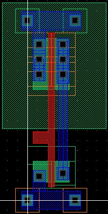
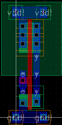
You have just finished the design of an inverter layout. You need to save
it by selecting Design -> Save. The layout view of the inverter
is shown below.
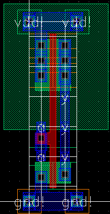
The next image shows the routing grid for the inverter to give you a better
idea of how the pins are placed along the intersectionsof the cell routing
grid. As you can see,
the origin of the cell (0.00,0.00) is located in the lower left-hand corner,
at the edge of the bounding box (this should be the case for all of your
standard cells).
You've just finished you first layout using ami06 technology. You can
finish this tutorial by exiting. Select
Window -> Close to exit layout editor, then in
CIW select Open -> Quit to quit Cadence.
Refer to 'Virtuoso Layout Editor User Guide' for more
information about layout editor.
Previous Tutorial
Main Menu
Next Tutorial