ABCPU2
Sketches of Logic Diagrams
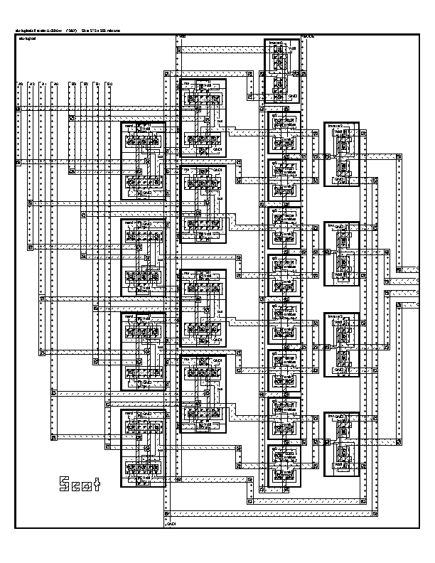
These sketches illustrate our early thoughts on the basic design of our
circuit. Most of these elements are in the final chip in some variation of
the form shown here. We have also provided Postscript versions of the final
logic for some of the more complex elements.
![[Inverter]](inverter.gif)
Simple CMOS Inverter
![[Transmission gate]](tg.gif)
CMOS transmission gate
![[NOR gate]](nor.gif)
NOR gate
![[XOR gate]](xor.gif)
XOR gate
![[Adder]](adder.gif)
Adder with carry
![[Arithmetic ALU]](alu-arith.gif)
Arithmetic ALU; M is mode bit (0 means add, 1 means subtract)
![[Logical ALU]](alu-logical.gif)
Logical ALU; M is mode bit (0 means and, 1 means or)
Also see the initial CIF file.
![[Accumulator Mux]](funkydiag.gif)
Accumulator multiplexor, which selects between loading from the ALU, loading
from the data bus, zeroing, circulating, or inverting for the accumulator.
(Postscript)
![[Address Generator]](addrgen.gif)
Address generator, which takes two separate 4-bit numbers from the data bus
and concatenates them into an 8-bit address.
(Postscript)
The program counter diagram is not inlined here due
to the size of the image. It is a loadable 8-bit ripple counter.
(Postscript)
We also have a sketch of the ALU; the real ALU is
implemented in exactly this fashion.
(Postscript).
For your amusement, we also provide a copy of our
original block diagram sketch.
Last modified 19 December 1996.