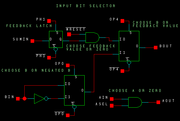
Several control signals dictate the operation of the arithmetic block:
The multi-functionality of the arithmetic block comes from taking several input bits and passing the appropriate two to the adder, based on the desired operation. The block accepts two numerical inputs from the data buses: A and B. Feedback within the block produces the previous arithmetic result (including carry-out) shifted right one bit.
An internal control signal ASEL is produced by ORing OP4 and the least significant bit (LSB) of the B input vector. This signal and control signals select the values to be passed to the A and B addition vectors, which will be processed by the carry lookahead adder described below.
These schematics may be used as a reference for the following descriptions of the individual operations.
OP4 is asserted, thus asserting ASEL. The A input vector (AIN) is passed to the A addition vector (AOUT). OP0 is deasserted, forcing a two-bit mux to pass the B input vector (BIN) to a second mux. OP4 causes the mux to pass BIN to the B addition vector (BOUT).
OP4 is asserted, thus asserting ASEL. AIN is passed to AOUT. OP0 is also asserted, forcing a two-bit mux to pass a bitwise-inverted version of BIN to the second mux. OP4 causes the second mux to pass BIN to BOUT.
OP4 is deasserted, thus the value of ASEL depends on the LSB of BIN. If that bit is asserted, then AIN is passed to AOUT. Otherwise, zeroes are passed to AOUT.
A feedback latch stores the shifted version of the previous addition result (SUMIN) on ph1. If MRESET is asserted, then SUMIN is ignored and zeroes are passed through the mux to BOUT. Otherwise, SUMIN is passed through the mux.
If the B input vector is shifted right one bit and the LSB of the output of the adder is stored on each cycle, then the full 16-bit result of the unsigned multiplication of the two 8-bit values A and B can be produced.
![]()
For our purposes, the simplicity of an 8-bit ripple-carry adder is far outweighed by its slowness, and the quickness of an 8-bit carry lookahead adder is far outweighed by its complexity. Our desire to implement a fast design and our space limitations resulted in the decision to serialize two 4-bit carry lookahead adders. The following description applies to a single 4-bit adder.
Central to the idea of the carry lookahead adder are the PG generators.
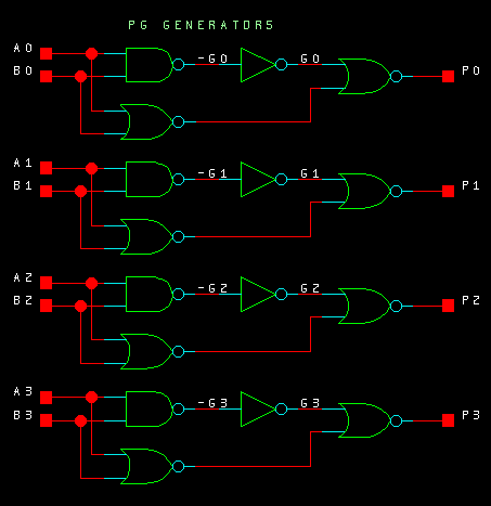
The P terms indicate whether the summation of two bits of the input will Propagate a carry bit. For example, if P2 is true, then if the carry-in (C1) to the summation of A2 and B2 is true, the carry-out (C2) will also true. Pn is the result of XORing An and Bn.
The G terms indicate whether the summation of two bits of the input will Generate a carry bit. For example, if G2 is true, the carry-out (C2) of the summation of A2 and B2 will be true regardless of the value of the carry-in (C1). Gn is the result of ANDing An and Bn.
The G bits (and their inverses, which are also needed) can be easily generated as intermediate values in the XOR gates used to generate the P bits.
The PG terms are used to generate the four carry terms.
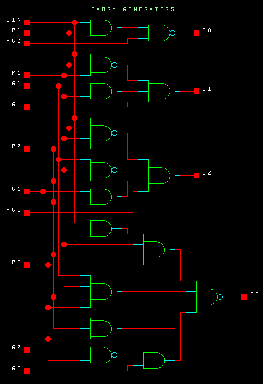
Each carry output is true if the associated generate bit is true, or if both the propagate bit and the previous carry output are true. Rather than actually use the previous carry bits in each case (which would not be far removed from a ripple-carry adder), the logic is expanded so that the four carry bits are generated in parallel.
The logic can be implemented more easily on a transistor-level as NANDs, as depicted in the schematics above.
The PG and carry terms are used to generate the sum terms.
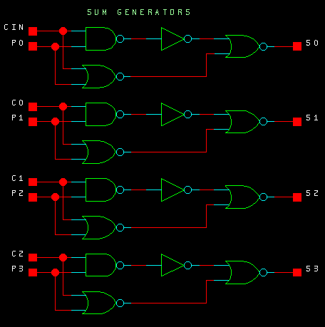
Each bit of the sum is an XOR of the associated inputs bits and the carry-in bit (the previous carry-out bit). The XOR of the inputs bits has already been calculated by the PG generator. Thus, only the XOR of each P bit with its carry-in needs to be found.
![]()
At the output of the adder are blocks which serve two purposes: drive the output bus when appropriate, and the latch the results for internal feedback.
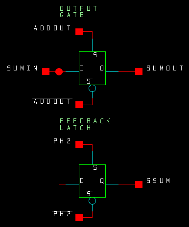
When ADDOUT is asserted, the arithmetic result (SUMIN) is passed to the output bus (SUMOUT). Otherwise, the arithmetic block does not drive bus.
SUMIN is latched on ph2, and the output of the latch is used internally to route the arithmetic results back to the input of the block for multiplication purposes, as described above.
![]()
The individual pieces described above can be combined to produce a single 8-bit adder/multiplier. For convenience, the input bit selectors and output gates/latches have been combined in 4-bit groups to match the adders.
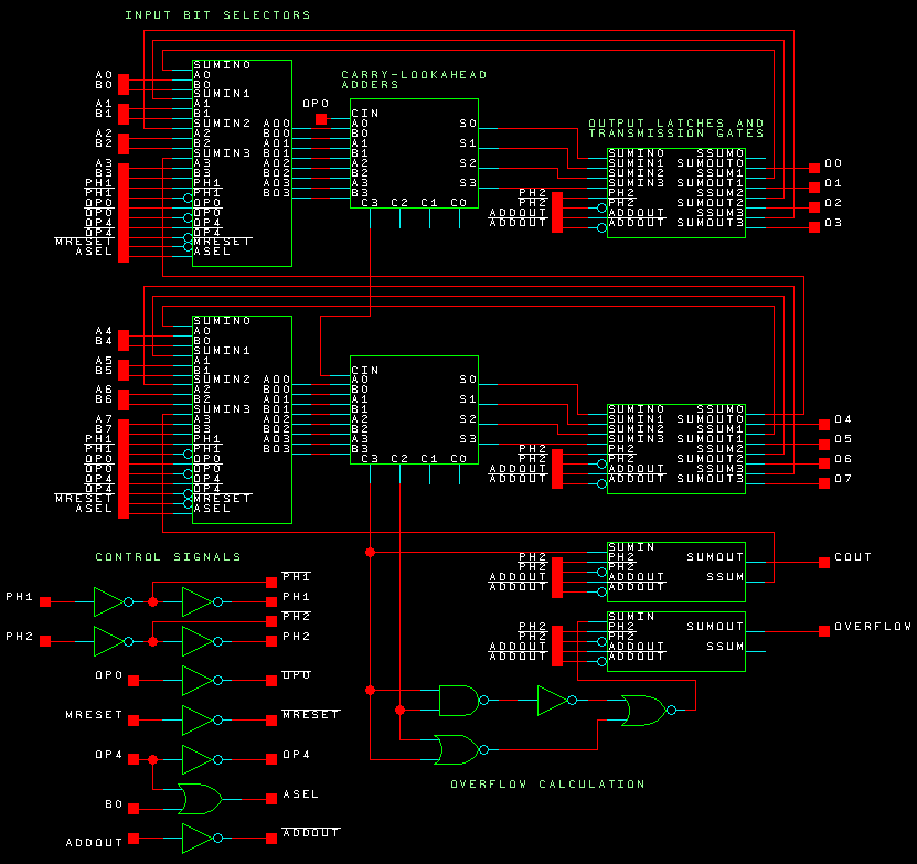
The inputs A and B are passed to the adders with a CIN of 0. The result is the two's complement addion of the two inputs.
The inputs A and a bitwise negated B are passed to the adders with a CIN of 1. The result is the two's complement subtraction of the two inputs.
The CIN to the adder is always 0. On the first cycle of a multiplication, the feedback sum is ignored. If B0 is 1, then the result of the addition will be the A input. Otherwise, the result will be zero. On subsequent cycle, one argument to the adder is A if B0 is 1 and otherwise. The other argument is the internal feedback value. low-order seven bits of the feedback value are the high-order seven bits the previous results, and the high-order bit of the feedback value is the previous carry-out.
A 16-bit self-shifting output register stores the final result and passes it to the output pads (see the section on latches). When the output latch is enabled, the data on the output bus is latched to OUT[15:8], and OUT[8:1] from the previous result is latched to OUT[7:0]. Thus, addition subtraction results are latched in the high-order eight bits of the output latch. For multiplication, the LSB of each partial product is stored by shifting it into the OUT7 as the new partial product is latched. On the final multiplication cycle, the first partial product is shifted into OUT0 as the last partial product is latched into OUT[15:8].
The inputs (A[7:0], B[7:0], OP0, OP4, MRESET, and ADDOUT) must be valid at the fall of ph1 and stable while ph2 is high (V1S2).
Supplementary latches (on ph1) are used to meet the timing constraints on the control signals MRESET and ADDOUT because the outputs of the control PLA are V2S1.
Calculation starts no later than the fall of ph1, and the output of the adder is valid by the fall of ph2. O[7:0] are latched on ph2 at the register. Internal latches (on ph2) are used for COUT and OVERFLOW because they are only driven by the adder, and thus all outputs (O[7:0], COUT, and OVERFLOW) are V2S1.
Feedback latches at the output of the adder latch on ph2, producing a V2S1 value. Corresponding latches at the input of the adder latch on ph1, producing a V1S2 value to satisfy the input constraints.