Functional Description
We have chosen to implement an 8-bit ALU/Calculator supporting a set of
standard arithmetic (two's complement), bitwise, boolean,
and shifting capabilities.
Key:
-
operation: The name of the operation.
-
operands: The number of operands the operation requires.
-
cycles: The number of cycles required to complete the operation. This
includes one cycle to read the opcode and one cycle for each operand that
must be read and latched. The output will always be available on the cycle
after the operation completes. A new opcode can be read on the same cycle.
Thus the last cycle of each operation may be overlapped with the first
cycle of the next one for higher throughput.
-
opcode: The 6-bit opcode value that the control unit recognizes for the
operation.
| operation |
operands |
cycles |
opcode (bin/hex) |
| Two's Complement Arithmetic |
| addition |
2 |
4 |
011000/18 |
| subtraction |
2 |
4 |
011001/19 |
| multiplication |
2 |
12 |
100000/20 |
| Boolean |
| identity |
1 |
3 |
000000/00 |
| nand |
2 |
4 |
000001/01 |
| nor |
2 |
4 |
000010/02 |
| xnor |
2 |
4 |
000011/03 |
| not |
1 |
3 |
000100/04 |
| and |
2 |
4 |
000101/05 |
| or |
2 |
4 |
000110/06 |
| xor |
2 |
4 |
000111/07 |
| Bitwise |
| identity |
1 |
3 |
001000/08 |
| nand |
2 |
4 |
001001/09 |
| nor |
2 |
4 |
001010/0A |
| xnor |
2 |
4 |
001011/0B |
| not |
1 |
3 |
001100/0C |
| and |
2 |
4 |
001101/0D |
| or |
2 |
4 |
001110/0E |
| xor |
2 |
4 |
001111/0F |
| Shifting |
| logical right shift |
2 |
4 |
010000/10 |
| arithmetic right shift |
2 |
4 |
010001/11 |
| rotate right |
2 |
4 |
010010/12 |
| logical left shift |
2 |
4 |
010100/14 |
| rotate left |
2 |
4 |
010110/16 |
The opcodes are selected to easily enable and control the operation of the
major blocks without decode-logic. For example, OP4 enables the
arithmetic block, and OP0 selects between addition and subtraction.
The following block diagram shows the basic data flow through the
ALU. The output flags are not shown.
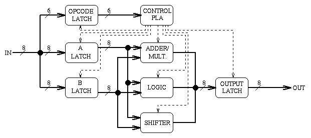
An 8-bit bus will receive input calculator-style: opcode on one cycle,
operand on the next, etc. Only 6 bits of the opcode will be latched and
decoded. A reset signal can be used to return the ALU to a clean initial
state and should remain de-asserted during normal operation.
A two-phase non-overlapping clock will synchronize events and
require less hardware than an edge-triggered single-clock ALU
implementation.
An 8-bit output will be used for the results of all
operations including multiplication, along with carry, overflow, ready,
and error flags.
The ALU will be composed of four basic blocks:
-
an adder block for addition, subtraction, and multiplication,
-
a logic block for bitwise and boolean operations,
-
a shifting block, and
-
a control unit composed of an automatically generated PLA.
These blocks are explained in further detail elsewhere.
-
Initial functional/interface design: Doherty, Morse, Pritchard
-
Opcode assignment: Doherty, Morse, Pritchard
-
Initial logic diagram: Doherty
-
Revised logic diagram: Pritchard
-
Webpage text/HTML: Pritchard