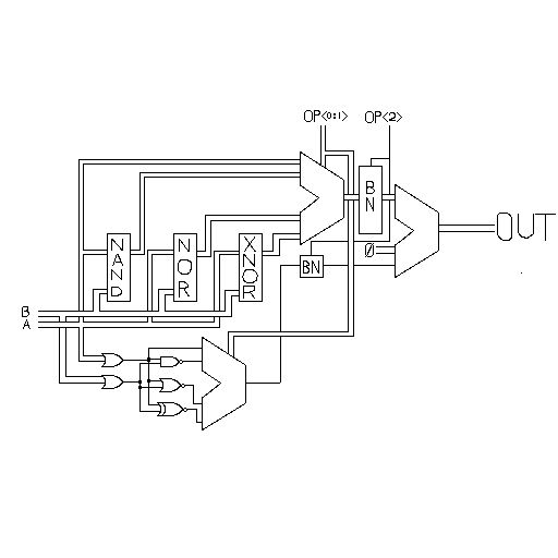
The layout of the logic block is fairly straightforward. The "bitwise" section of the layout, which handles the bit-by-bit operations, consists first of a nand gate, a nor gate, and an xnor gate, which are connected with a and b as inputs. Then, the three gate results are multiplexed with the value of a, using op0 and op1 to select as necessary. Then, these signals are multiplexed with their inverse using op2. For the "boolean" (i.e., C-style boolean) functions, the a and b inputs are or'ed together and fed to a set of logic identical to the above. Finally, the low bit of the output is produced by muxing the low bit of the "bitwise" functions with the "boolean" output bit. As for the top 7 bits, the "bitwise" outputs are AND'ed with op3 to ensure that they are only on for "bitwise" functions.
The signals which control the action of the logic block are:

All signals entering the block, which are a[7:0], b[7:0], op[3:0], and LOGICOUT, are V1S2. Since the block is purely combinational, the output is also V1S2.
The results of simulating the logic block with an irsim command file can be viewed in two sections: 1, 2.
The block was tested with an 8-bit latch connected to the output to truly test the operation from the output of the ph1 latches driving the block to the output of the ph2 latches it drives. A crystal command file was used to find critical path data.
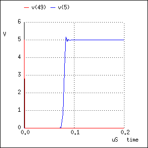
As you can see from scanning the crystal output, it predicts a worst-case path of 122.67 ns through the logic block, the critical path for the whole chip. Spice simulation yielded the following graph:
red v(49)=a5
blue v(5)=out0

The graph indicates that the time through the logic block is closer to 90 ns, which allows easily for a 5 MHz operation.