The registers are quite straightforward. The A and OP registers are simple 8-bit latches with a control signal to control when latching occurs. The B register takes the original 8-bit latch and adds another 8-bit latch, along with a second control signal to control whether new data is latched into B or [GND,B[7:1]] is latched.
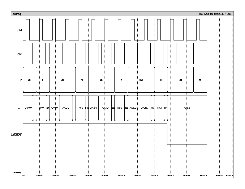
Similarly to B, the OUT register starts out as a simple 16-bit latch, but adds an 8-bit latch, so that OUT[15:8] latches whatever is fed to it, while OUT[7:0] latches OUT[8:1].
The A, OP, and OUT registers each accept a signal called LATCHregname where regname is the name of the registers. This signal tells the register to go ahead and latch instead of holding its previous value.
The B register accepts two control signals: LATCHB and LOADB. LATCHB is similar to the latch signals above. LOADB selects the input for the latches from between the contents of the input bus and [GND,B[7:1]].
![]()
![]()
![]()
![]()
Each register was simulated using irsim. Here are the results:
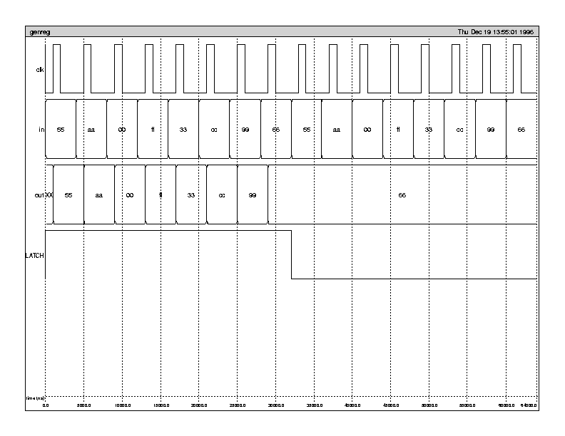
The above simulation results are also available in .ps format.
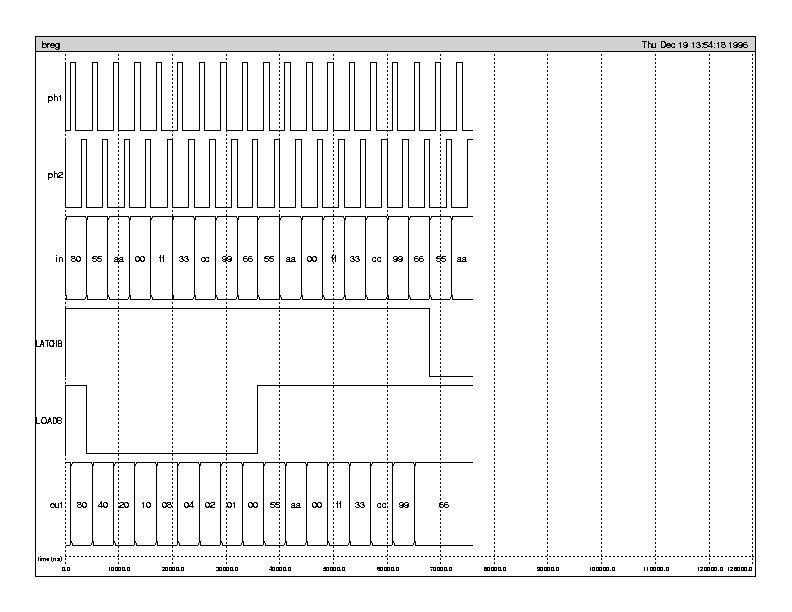
The above simulation results are also available in .ps format.
The above simulation results are also available in .ps format.
The above simulation results are also available in .ps format.
We decided not to do any timing analysis on the registers since there really was no possibility that the critical path for the circuit would be found there.