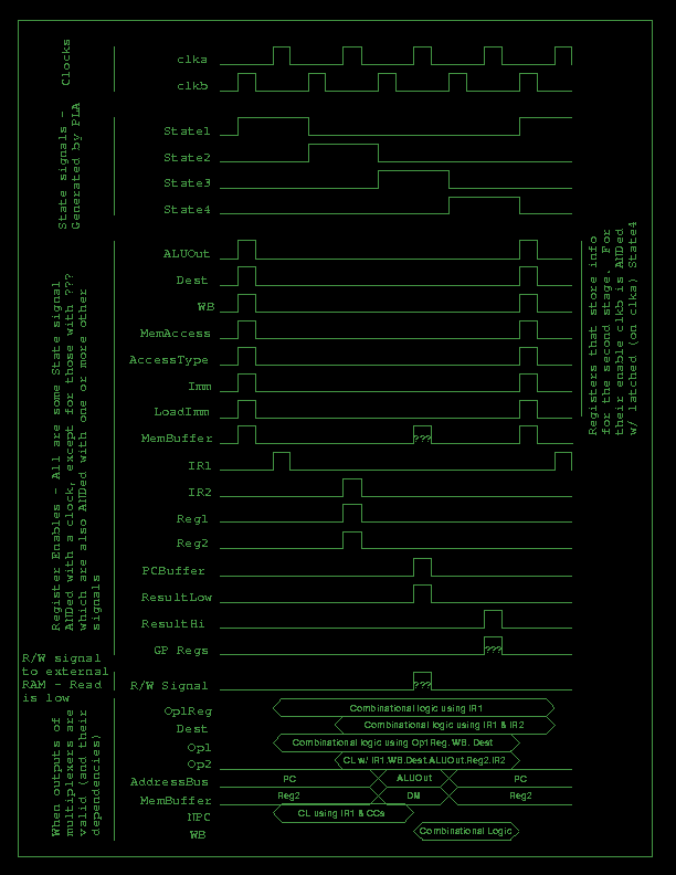
The following is a timing diagram for the
processor showing clocks, PLA outputs, register enables, and when multiplexer
outputs are stable. Those registers used to hold information during the second
stage are all enabled during clkb. State4 (an output from the PLA) is latched
on clka, and this is ANDed with clkb to provide the enable for those registers.
This means that the very first instruction executed (when the processor leaves
the initialization state) will not have bogus information stored in those
registers. However, some will have to be latches with clear inputs (they
will be cleared during initialization as before), as will the PC.
There are a few signals with ??? below. These refer to signals that may be
enabled as shown, but this enable is ANDed with one or more other signals.
In particular, MemBuffer enable is anded with MemAccess and AccessType==LOAD
and the general purpose registers (GP Regs) enable is ANDed with WB. Note that
R/W is always READ (low) except during State3 * clka it will be
WRITE (high) if MemAccess and AccessType==STORE.
Also, there is one multiplexer not shown, the ALUop. It has the same
timing as Dest (i.e. stable as soon as IR1 and IR2 have been latched), which
is in time for the ALU to perform its calculation.