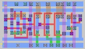

Four clearable latches make up the PC Register so that upon RESTART (at a Loading mode), CLEARPC is asserted and the 4 bits of the PC Register becomes zero (0000). At this point, we will start prefetching instructions and storing them into the IM Storage. The first instruction is stored in the IM Storage location 0000. Once the CPU is done storing the first instruction, LDPCBUF is asserted by the PLA, loading the current PC value (0000) into the PC Buffer. The PC Buffer is directly connected to the PC Adder, which is a combinational logic that adds up two numbers--from the PC Buffer and the MUX, respectively. The MUX chooses between a hard-wired logic ONE (0001) and the 4-bit input from the BUS. During a regular cycle, the BRANCH signal is 0, so the MUX passes the hard-wired logic ONE to the PC Adder. However, during a BRANCH instruction, the BRANCH signal is asserted high by the PLA and the MUX passes the 4-bit BUS value to the PC Adder instead.
In the cycle after the PC Adder has added up the two numbers, the PLA asserts WRITEIM to write the BUS value to the IM Storage location that is currently indicated in the PC Register (0000). The cycle after that, INCPC is asserted by the PLA and the value in the new value in the PC Adder (0001) is latched to the PC Register.
This process repeats during the Loading stage, until the value of the PC Register reaches ten (1010). The PC Register bits are connected to a PC Check unit. The PC Check unit is hard-wired to test for the pattern 0101. Once it detects a 0101, indicating that the CPU is done loading all ten Instruction Memory Storage locations, the PC Check asserts the LOADDONE signal, telling the PLA to change from the Loading mode to the Running mode.
The Segmentation Fault Detector is a 4-bit input decoder that checks to make sure the PC value is less than or equal to ten. If the PC value exceeds ten, IMSEG is asserted, indicating that IM has encountered a segmentation fault.
The output from the PC Decoder asserts one of the memory locations' READ or WRITE signal. When the WRITE signal of an IM Storage location is asserted, the value in the INBUF is written into that memory location. On the other hand, when the READ signal of an IM Storage location is asserted, the value from that storage location is read to the OUTBUF.PC Unit
The PC Unit is composed of 6 sub-units: MUX, PC Buffer, PC Adder, PC Register, PC Check, and Segmentation Fault Detector. The main function of the PC Unit is to keep track of the address of IM Storage locations. PC Decoder
The PC Decoder takes the 4 PC bits as inputs along with the READIM and WRITEIM signals generated by the PLA. It decodes those 6 inputs into one of its 20 outputs--READ or WRITE signals for each of the ten IM Storage locations.INBUF
The INBUF is an interface between the IN Register (not in the IM Unit) and the IM Storage. When LDIMBUFLO is asserted by the PLA during the loading stage, INBUF stores the 4 bits that come from the IN Register into the lower 4 bits of the INBUF. These 4 bits are the OPCODE bits. During the next clock cycle when the PLA asserts LDIMBUFHI, the 4 bits from the IN Register are stored in the upper 4 bits of the INBUF. These are the OPERAND bits.IM Storage
The IM Storage consists of ten 8-bit storage locations. Each of the bits in the IM Storage is a static latch cell with an extra safety inverter and an extra safety transmission gate to assure that the value inside the latch cell will not be corrupted by whatever is on the bus. This IM latch cell is shown in the following figure: A Latch Cell of the IM Storage.