See our Timing Diagram. Or keep reading to see
how we set up the timing of our circuit to ensure that it would work.
Terminology
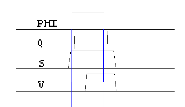
Signals are divided into 4 types, characterized by their duration. A clock
pulse is the basis, called Phi. A signal of the same length as the clock,
created by ANDing it with Phi signal, is Qaulified.
Stable signals are defined before the pulse goes high and after
the pulse goes low. On the other hand, Valid signals are only
defined as the clock goes low.
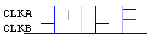
Two-Phase Clocking System
In order to prevent clock races, the PLA generates signals based on two non
overlapping clocks.
The state changes based on inputs that must at least
VA. Then, outputs change with the state with clockB and
are VBSA.
Timing Requirements
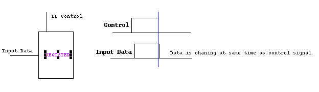
All register control signals come from the PLA and are
VBSA. For loading, the control signal needs
to be more precise, so a Qualified signal is used. ANDing with
clockA creates a QA. Then, since the data is loaded on
the falling edge of clockA, the input must be at least
VA.
This means that whenever data is transfered from one register to another,
e.g. via the bus, the output must provide VA signals.
The simplest method for doing this, given a
VBSA control, is to enable the register to
drive the bus for the duration of the control. Thus, the input the
recieving register is at least SA, longer than
necessary.
Notice that if the driving control were Qualified, the
QA input data would be changing at the same time the
control edge was falling, causing a timing hazard.
The following figure shows that our system meets the above requirents for loading
the IM and executing a sample instruction, ADD. Other instructions have
similar timings. Timing Diagram