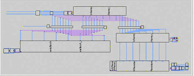
The Output section contains a serial loaded latch that gets inputs from the adder and shifts in a new bit every clock cycle. The shift register is used for both multiply and divide and can be flipped to output either the top or bottom bit as the MSB on the output pin. The output array also contains latches for the feedback paths between the adder and the input stages.