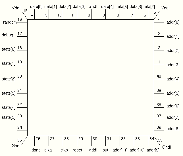
- addr[3]
- addr[2]
- addr[1]
- addr[0]
- Vdd
- data[0]
- data[1]
- data[2]
- data[3]
- Gnd
- data[4]
- data[5]
- data[6]
- data[7]
- Vdd
- random
- debug
- state[0]
- state[1]
- state[2]
- state[3]
- state[4]
- state[5]
- unused
- Gnd
- done
- clka
- clkb
- reset
- Vdd
- out
- addr[11]
- addr[10]
- addr[9]
- addr[8]
- addr[7]
- addr[6]
- addr[5]
- addr[4]
- Vdd, GND - For delivering the juice!
- clka, clkb - We march to the beat of a different drummer
- reset - To be asserted on power-up and when you want to start
over
- data[0:7] - For receiving data from the SRAM, or for addressing
the register file while in debug mode (see the debug
signal below)
- random - This should change randomly on every clock cycle
- debug - While this is asserted, the PLA is paused and
data[0:6] can be used for random access to the
register file
- addr[0:11] - Output pins for addressing the off-chip SRAM
- state[0:5] - Outputs for debugging (the state bits from the master
PLA)
- done - Asserted when we have the solution! When done is
high, the register file can be addressed using
data[0:6] (just like in debug mode)
- out - This is where the data goes when you address the
register file through data[0:6]