Back
Main Menu
The Routing Grid in 0.5µm Library
This document is an FYI introduction to the routing grid and cell boundry
conventions for the 0.5µm standard cell library. If you want to use the
auto-routing capability of Cadence, your cells need to be designed following
these conventions.
The grid we are using is more conservative than others to limit resource
usage during place&route and to give us flexibility in the cell design.
All metal spacings are via-to-via and also allow for diagonal vias. This
means that vias can be placed on any two adjacent grid points without DRC
violations. Although the grid will be slightly wider that way, it makes
routing much easier. The SCMOS_SUBM rules define the following layer spacings:
- via1 to via1: 3 lamba
- via2 to via2: 5 lambda
- metal1 to metal1: 3 lambda
- metal2 to metal2: 3 lambda
- metal3 to metal3: 4 lambda
- metal1 minimum width: 3 lambda
- metal2 minimum width: 3 lambda
- metal3 minimum width: 5 lambda
This would mean the following minimum grid widths:
- metal1: 7 lambda
- metal2: 8 lambda
- metal3: 10 lambda
Since we are using a horizontal- vertical- horizontal routing scheme we will
route both metal1 and metal3 horizontally. For the horizontal grid we choose
the larger of the two minimum spacing values for metal1 and matal3 (the two
horizontal layers) and for the vertical grid we simply use the minimum spacing
value for the vertical layer, metal2. This grid allows stacked vias at every
intersection on the grid. To give us more flexibility in the design we also
introduce an offset of half the grid spacing. The following drawing summarizes
all routing grid dimensions, note that the green line symbolizes the actual
cell boundary that we will use later in abstract generation:
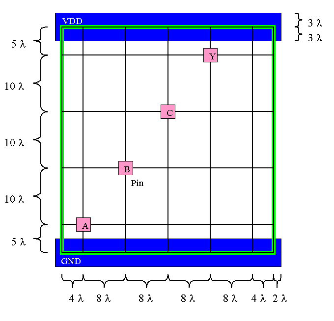
Power supply rails
Since every second row will be flipped, only half of each rail belongs
to one cell. With the 6 lambda width we use, 3 lambda fall inside the cell
boundary. To ensure DRC compliance at the row ends, there is also a 2 lambda
overlap to the right and left. Be sure to draw the supply exactly as shown.
The cell boundary later in abstract will be extracted based on the metal1
shapes in the supply rails.
Pin Placement
All pins must be placed on intersecting routing grid points. WRoute (Silicon
Ensemble's router) is capable of routing off-grid, however according to
Cadence this is highly discouraged. In addition, pins should be staggered
whenever possible. This will allow WRoute to access pins either horizontally
or vertically without one pin blocking others.
Metal2 usage
In our HVH routing scheme metal2 is the most constrained layer.
Care should be taken not to block metal2 tracks (route as much as possible
in poly and metal1). If metal2 has to be used, it should only run vertically
and fully within one routing track, so only one track inside the cell is blocked.
Back
Main Menu