ELEC 241 Lab
Design
Looking at the diagram of our system
in Figure 9.2
we already have some of the components that we need:
The mixer amplifier from Experiment 4.3
will convert the acoustic source signal to an electrical
signal,
and the earphone amplifier from Experiment 6.2
will convert the received electrical signal back to
an acoustic signal.
That leaves just the transmitter, antennas (to interface to
the wireless channel) and the receiver.
Part A: The Transmitter
The function of the transmitter is defined by the equation
$$x(t)=A_c\bigl(1+m(t)\bigr)\cdot\cos(2\pi f_ct)$$
If we dissect this equation, we can identify the following
five
things we need to do
-
Generate the
source signal \(m(t)\).
(We've already done this with the microphone and mixer
amplifier.)
-
Add one.
(We can do this with an op-amp.)
-
Generate the carrier signal \(\cos(2\pi f_ct)\).
(We can do this with the function generator.)
-
Multiply the carrier signal by \(1+m(t)\).
(We don't know how to do this with an op-amp.)
-
Multiply by \(A_c\).
(Depending on \(f_c\) and \(A_c\) we may or may not be able to do this with an op amp.)
Unfortunately, the one thing we can't do with an op-amp
(step 4) is the core of the modulation process.
In fact, multiplying two signals is challenging
regardless of the circuit components we have available.
Fortunately, multiplying two numbers is a trivial operation
for a computer, so if we're willing to use
the computer as
part
of our system,
we can proceed.
Part B: Choice of Carrier Frequency
Since the maximum sampling rate of our D/A converter is
\(f_s=1.25~\text{MHz}\), the maximum carrier frequency we can use
is \(f_s/2=625~\text{kHz}\).
If we consult
Part 15
of the FCC regulations, we find the only frequencies in this range
where we can legally transmit significant amounts of power
are in the
\(160-190~\text{kHz}\) band.
Part C: Antennas
The down side of using frequencies in the \(160-190~\text{kHz}\) band
is that the wavelengths are long (greater than \(1.5~\text{km}\)).
Since an efficient antenna has to be on the order of the wavelength,
we are restricted to using antennas which are very inefficient.
For a simple antenna we have two choices:
an electric antenna,
which is basically a long piece of wire
(like the radio antenna on your car)
or a magnetic antenna, which is simply a coil of wire.
Since we can increase the effective size of a magnetic antenna
without increasing the physical size by adding additional
turns to the coil, we will choose a magnetic antenna.
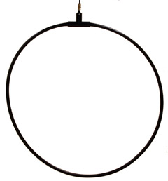
The antenna we will use consists of 8 turns of wire in
a loop of diameter 65 cm.
Part D: The Receiver
The optimum (coherent) AM receiver is shown in Figure 9.4 in
the previous section.
The core of this receiver is nearly identical to that of the
transmitter: the received signal is multiplied by a sinusoid
at the carrier frequency.
In addition, the received signal is bandpass filtered to
reduce noise and the demodulated signal is lowpass
filtered to eliminate the copy centered at \(2f_c\).
As with the transmitter, we will have to use
the computer
to
multiply the received signal by the carrier.
Since we can build much better filters digitally than we
can with analog circuits, we'll do the filtering portion of
our receiver in Labview as well.
Here's the list of required receiver functions:
-
Bandpass filter \(r(t)\) to produce \(\tilde{r}(t)\).
-
Generate the carrier signal \(\cos(2\pi f_ct)\).
-
Compute \(\tilde{r}(t)\cos(2\pi f_ct)\).
-
Lowpass filter to produce \(\widehat{m}(t)\).
Part E: Antenna Interface Module
We've completed most of the hard part of the design,
at least in terms of signal processing,
now all we need to do is connect them
all
together.
Here's a list of the remaining tasks:
-
Connect the transmitter and receiver to the antenna.
-
Since the transmitter and receiver share a single antenna,
we need a way to switch between them.
-
Because of the low efficiency of
the transmitter
antenna,
we need a large amount of
electrical
power to produce a radiated
EM wave of usable strength.
I.e.
the transmitter requires
an amplifier with high power gain.
-
Similarly, the low efficiency of
the receiver
antenna means that even a strong EM wave
will produce a small electrical signal.
We should also amplify the received signal
before processing it.
-
To improve the effective efficiency of the antenna,
we should match its impedance to that of the amplifiers.
-
Since we will be using DSP for our signal processing,
we should lowpass filter the received signal to prevent aliasing
and the transmitted signal to remove harmonics.
Given that there are only
four
more weeks in the semester
and that we
need to learn Labview before we can do the hard part,
it might be a good idea to outsource this last Part
of the design.
Fortunately, there's an empty spot on the breadboard
where we can install an additional Interface Module.
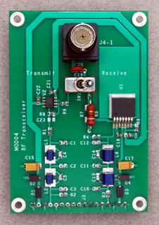
The circuit below provides the necessary functions:
 Click to enlarge.
Here's how it works:
-
Capacitors C10-C12, inductors L5 and L6,
and resistors R3 and R4
form the lowpass filter for the transmitter signal.
This is a 5th order elliptic filter with a
250 kHz cutoff frequency.
-
The filtered transmitter signal is connected to the input of
U1,
an
LMH6321 300 mA high speed buffer.
This is basically a high power, wide bandwidth op amp
wired as a unity gain buffer.
-
With
SW1 in the lower position, the output of U1 is connected to the
antenna through C20 (C19 is not installed).
C20 cancels the inductive component of the antenna impedance
to provide a more efficient power transfer.
-
With SW1 in the upper position,
the antenna is connected to the input of the circuit
consisting of U2, R8, R9, and C23.
U2 is an
LM7171 high speed op-amp.
-
Capacitors C1-C5, inductors L1 and L2, and resistors R1 and R2
form another 5th order elliptic lowpass filter
with a 250 kHz cutoff.
This
helps to reduce
aliasing when the amplified receiver signal is
digitized.
Here's what it looks like:
 Make sure that the antenna module is installed on your
breadboard when you're ready to use it.
Talk to your labbies or Mr. Randy Fly if
you don't already have one on your board.
The connection for the transmitter
is on
pin 39
of the interface connector
and the connection for the receiver is on
pin 29.
Make sure that the antenna module is installed on your
breadboard when you're ready to use it.
Talk to your labbies or Mr. Randy Fly if
you don't already have one on your board.
The connection for the transmitter
is on
pin 39
of the interface connector
and the connection for the receiver is on
pin 29.