Let's apply our new Labview skills to
the task of improving
the resistance/temperature
measurement system we built last week.
| |
|

|
Step 1: |
|
Restore the connections you had in
Experiment 3.2 last week
with
the 0-6 V output of the power supply (set to 5.00 V)
connected to J1-3.
Check that the circuit on your breadboard is still wired correctly.
Load and run the VI you saved last week and verify that it still
produces the correct reading for temperature.
Vary the power supply voltage and observe that the temperature
reading changes in response.
|
Step 2: |
|
Stop the VI.
On your breadboard, add a wire to connect  to
ach4,
so that your circuit looks like this:
to
ach4,
so that your circuit looks like this:
![\includegraphics[scale=0.500000]{ckt3.3.5.ps}](img229.png)
|
Step 3: |
|
We are now asking the A/D converter to read two different
voltages simultaneously. This is not a problem for the A/D
converter, but it does require
us
to figure out how Labview represents multiple simultaneous samples.
The obvious way to handle this would be to simply add another A/D
block and set it to A/D Channel 4.
If you try this, you will get a cryptic error message to the
effect that the device is already in use. This is because all of
the channels are on the same card, and the first channel which is
opened has exclusive use of the device.
Labview handles this by combing multiple samples into a
vector,
with one entry for each channel.
Double click the A/D block or select
Properties
from the menu.
This will bring up the
DAQ Assistant
dialog.
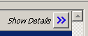
Click on the
Show Details
button near the top of the panel
|
Step 4: |
|
Click on the
Add Channels
button.
 Select
Voltage
from the popup menu,
then select
ai4
from the list of Supported Physical Channels.
A new entry for ai4 should appear in the channels list.
Note the
Scan Order
column.
This tells us that channel 5 will be the first element of the
vector of samples and channel 4 will be the second.
Although this seems untidy, it won't cause problems
as long as we remember the order.
Click
OK
and wait until everything has settled down.
Select
Voltage
from the popup menu,
then select
ai4
from the list of Supported Physical Channels.
A new entry for ai4 should appear in the channels list.
Note the
Scan Order
column.
This tells us that channel 5 will be the first element of the
vector of samples and channel 4 will be the second.
Although this seems untidy, it won't cause problems
as long as we remember the order.
Click
OK
and wait until everything has settled down.
|
Step 5: |
|
The block diagram looks the same as before, but now the wire
is carrying two separate values.
Perhaps surprisingly, this fact does not change the original
operation of the VI.
Subsequent blocks, expecting a single value, simply take the first
element of the vector.
Since we left the original signal
( ) as the first element, everything to the right of the
A/D converter block works as it did before.
Start the VI and verify that this is the case.
) as the first element, everything to the right of the
A/D converter block works as it did before.
Start the VI and verify that this is the case.
|
Step 6: |
|
If we know how to look, we can see that the wire coming out
of the A/D converter block is in fact carying two values.
With the VI still runing, bring the block diagram window to
the top.
Place the cursor over the wire between the
DAQ Assistant
block and the numeric indicator labeled
VT.
The wire should start flashing and the cursor will turn into
a circle with the letter "P" in it.
This is the symbol for a
probe.
Left click to place the probe.
A small rectangle labeled
1
will appear at the output of the A/D converter block
 and a window labeled
[1] data
will pop up.
and a window labeled
[1] data
will pop up.
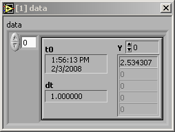 The probe display window
shows the value of the data on the probed wire.
The numeric control in the upper left corner
(currently zero) determines
which of the wire's signals is displayed.
Type "1" into this field or click on the upper arrow to
the left of the box.
The value displayed for
Y
should change to a value close to 5.
The probe display window
shows the value of the data on the probed wire.
The numeric control in the upper left corner
(currently zero) determines
which of the wire's signals is displayed.
Type "1" into this field or click on the upper arrow to
the left of the box.
The value displayed for
Y
should change to a value close to 5.
|
Step 7: |
|
Stop the VI.
Widen the block diagram window, or scroll it to create some
empty space to the left of the while loop.
Place the cursor on the border of the while loop.
Resize handles (small black squares) should appear.
Place the cursor over the one in the center of the left edge
and widen the while loop by about an inch.
move the
DAQ Assistant
near the left edge of the loop.
|
Step 8: |
|
Click on the wire segment coming out of the
data
terminal of the
DAQ Assistant
block
and press
Delete
to remove it.
The remainder of the wire will become broken,
since there is now no input.
From the
Functions
palette, select
Sig Manip,
then
Split Signals.
Place the resulting icon between the
A/D converter output and the leftmost
portion of the broken wire, and click to release.
The split signals block is expandable to accomodate the
number of signals in a bundle.
Place the cursor over the middle of the bottom edge and
move it around until it turns into a resize arrow.
Drag the bottom edge down by one increment.
The resulting icon will look like a wishbone in a box.

|
Step 9: |
|
Wire the left side
of the split signals block
to the A/D output.
The upper output is
(ach5).
Connect it to the broken
wire.
|
Step 10: |
|
The lower output is
, which will replace
the constant value of 5 currently connected to
the upper input of the subtract block.
Delete this numeric constant block and wire the
lower output of the split signal block
to its previous destination.
|
Step 11: |
|
Start the VI and verify that the displayed temperature value is still correct.
Vary the value of
and verify that it remains correct.
|
Much of what we will do in subsequent Labs,
especially Labs 7 and 8,
will be devoted to minimizing the effect of noise.
For now we will content ourselves with the most common
response to unwanted variation in data:
taking the average.
| |
|
|
Step 1: |
|
Before we start to improve the situation, let's try to get
a quantitative idea of how bad it is.
At the moment what we know is that the displayed value
jumps around a lot. Let's get a picture of those jumps.
Stop the VI and go to the front panel.
Right click to bring up the
Controls
palette, go to
Graph Inds,
and select
Chart
from the
Graph Indicators
palette.
Place the resulting chart in a convenient location on the
front panel.
|
Step 2: |
|
Use
Find Terminal
or your own navigational skills to find the
icon for the
Waveform Chart
on the block diagram.
Position it directly above the icon for the
VT
numeric indicator.
Connect its input to the
T
output of the formula node.
|
Step 3: |
|
Return to the front panel and start the VI.
The chart will provide a graphic record of the variations
in the temperature reading.
Accumulate about a minute's worth of readings,
then stop the VI and make a printout of the front panel.
|
Step 4: |
|
Go to the block diagram and widen the left-hand of the while
loop by about 1.5 inch.
Move the
DAQ Assistant
block to the left edge of the while loop.
Disconnect the
data
output of the
DAQ Assistant
block from the input of the
split signals block.
|
Step 5: |
|
Right click to bring up the
Functions
palette, select
Analysis,
then
Statistics.
Place the resulting block between the
DAQ Assistant
block and the split signals
block.
When the
Configure Statistics
dialog appears, select
Arithmetic mean,
then click
OK.
Connect the output of the
DAQ Assistant
block to the
Signals
input of the
Statistics
block.
Connect the
Arithmetic Mean
output to the input of the split signals block.
|
Step 6: |
|
If we were to run the VI at this point, we would get
the same behavior as before.
This shouldn't be surprising, since the average of
a single value (the
1 Sample
from the
A/D converter)
is just the
original value.
What we need to do is take the average of a large number of
input values to produce a single output.
Double click on the
DAQ Assistant
block to bring up the configuration dialog.
Under
Acquisition Mode,
change
1 Sample (On Demand)
to
N Samples.
Under
Clock Settings,
set
Samples To Read
to 1000.
Since the
Rate
is 1000 samples per second, this will give us 1000
values to average.
Click
OK.
|
Step 7: |
|
Since the process of gathering the 1000 samples now consumes
one second, the
Time Delay
block is no longer needed.
Either delete it, or edit it and set the delay to zero.
|
Step 8: |
|
Return to the front panel and start the VI.
The signal on the
Waveform Chart
should be much smoother.
In fact we might be willing to believe that the variations
that remain correspond to actual changes in temperature.
Save a minute of new data and print a copy to compare
with the unsmoothed plot.
|
Step 9: |
|
Stop the VI and save it in a persistent location.
|
| |
|
|
Step 1: |
|
In the circuit from the previous Part,
replace the thermistor with your CdS photocell.
|
Step 2: |
|
Make a copy of the
VI you used in the previous part and give it an appropriate name.
Load this VI and go to the block diagram.
|
Step 3: |
|
Based on the information in the CdS photocell data sheet,
derive a formula which gives the illumination level (in Lux)
in terms of the resistance.
|
Question 1: |
|
Summarize your derivation in a form that will convince both
you and your labbie of its correctness.
|
Step 4: |
|
Replace the formula in the formula node of the block
diagram with the one you derived in the previous step.
On the front panel, change the label of the temperature
display from
T
to
Illumination.
|
Step 5: |
|
Since light can vary much more rapidly than temperature,
the
Waveform Chart
display would be more useful with a faster update rate.
Edit the A/D converter block and change the
Samples To Read
from 1000 to 100.
|
Step 6: |
|
Start the VI and verify that it works correctly.
|
Step 7: |
|
Determine the illumination level under various conditions:
under-shelf flourescent lamp on or off, incandescent lamp
on or off, photocell shaded by lab notebook, etc.
If necessary,
clear the plot by right-clicking over the display window
and selecting
"Clear Chart".
|
Step 8: |
|
Turn off the incandescent lamp and under-shelf flourescent lamp.
Clear the plot.
Observe changes in the illumination seen by the photocell
as people move around in the vicintity of the lab station.
|
Question 2: |
|
Suggest how the information in the illumination vs. time
plot could be used in an intrusion detector.
|
Step 9: |
|
Set the (old-fashioned, analog) function generator
to produce a 1 Hz, 8 V p-p square wave.
Use BNC clip leads to connect a red LED to the
50 Ω
Output
(polarity is not important).
The LED should be flashing at a rate of once per second.
|
Step 10: |
|
Hold the LED over the photocell, pointing downward.
Observe the resulting waveform on the
Waveform Chart
display.
Increase the distance between the LED and the photocell
and note the maximum distance at which the signal from
the LED is still discernable in the displayed waveform.
|
Remark: |
|
The last step provides an example of an optical
communication system where the signal delivered
to the LED is transfered over an optical channel
to emerge (somewhat the worse for wear) some distance
away as the output of the photocell.
This is essentially the same arrangement we used
in Part 3 of Experiment 2.3, except we're using
the photocell instead of the photodiode.
The response of the photodiode is much faster
than that of the photocell,
but we found that its output voltage was a distorted
version of the optical input.
The I-V plot we made for the photodiode in Experiment
4.3 suggests the reason for this:
viewed as a
current
source the photodiode's output is linear in
the input irradiance, while viewed as a
voltage
source its output is logarithmic.
We will deal with this next week by building
a cicruit which converts this output current to a voltage.
|
![\includegraphics[scale=0.500000]{ckt4.2.2.ps}](img230.png)