![\includegraphics[scale=0.500000]{ckt3.3.4.ps}](img228.png)
In previous Labs we have developed a number of different interfaces to resistive sensors. In Lab 1 we simply connected the sensor to the DMM. This is quick, but not suitable for use with Labview. In Lab 3 we achieved Labview compatability with this circuit:
![\includegraphics[scale=0.500000]{ckt4.2.2.ps}](img230.png)
As we saw in Lab 4, this circuit gives good results with the thermistor and CdS photocell. These devices, especially the photocell, are characterized by producing significant changes in resistance in response to the measurements we wished to make. However, other types of sensors, such as strain gages, produce very small changes of resistance. If we use this circuit with such sensors, it can severely limit the precision of our measurements.
Let's consider a simplified version of the two circuits shown above.
![\includegraphics[scale=0.500000]{ckt8.0.1.ps}](img238.png)
When drawn this way, the circuit looks like a voltage
divider, so
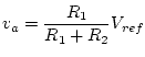 If we consider the sensitivity of the output voltage
 ![]() to changes in the sensor resistance
to changes in the sensor resistance ![]() , we get
, we get
 .
For small changes (
.
For small changes (![]() ) in
) in ![]() the corresponding change
in
the corresponding change
in ![]() is
is
 If
If ![]() is the nominal value of the sensor resistance and we
choose
is the nominal value of the sensor resistance and we
choose ![]() , then
, then
 .
.
As we saw in the Introduction to Lab 5,
the minimum resolvable step for the A/D converter on the 10 V
range is 0.31 mV.
This means that the smallest change in resistance that we can
measure is
 or about 0.012%.
This doesn't seem like much of a limitation, but the pressure
sensor we will be using in Experiment 8.1 has a full-scale
resistance change of only 0.25%, which would give
us a resolution of only 1/20 full-scale.
or about 0.012%.
This doesn't seem like much of a limitation, but the pressure
sensor we will be using in Experiment 8.1 has a full-scale
resistance change of only 0.25%, which would give
us a resolution of only 1/20 full-scale.
The root of the problem is that the total change in the voltage
![]() is only a small fraction of the range of the A/D converter.
But since this value is located in the middle of the range,
we can't amplify
is only a small fraction of the range of the A/D converter.
But since this value is located in the middle of the range,
we can't amplify ![]() without exceeding the range of the
A/D converter.
What we need to do is amplify the
changes
in
without exceeding the range of the
A/D converter.
What we need to do is amplify the
changes
in ![]() about its nominal value.
about its nominal value.
Suppose that we add a second voltage divider to the above circuit:
![\includegraphics[scale=0.500000]{ckt8.0.2.ps}](img239.png)
![\includegraphics[scale=0.500000]{ckt8.0.5.ps}](img240.png)
We already have a circuit that will
amplify ![]() ,
the difference amplifier we saw in Part 4
of Experiment 5.2:
,
the difference amplifier we saw in Part 4
of Experiment 5.2:
![\includegraphics[scale=0.500000]{opamps/diff2.ps}](img237.png)
![\includegraphics[scale=0.500000]{ckt8.0.3.ps}](img241.png)
Recall that in Part 4 of Experiment 5.2 we showed that
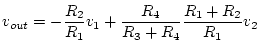 .
If
.
If
![]() and
and ![]() , then
, then
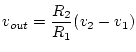 .
But if the resistances aren't exactly matched, we will have
different gains for the inverting and non inverting inputs.
Suppose that
.
But if the resistances aren't exactly matched, we will have
different gains for the inverting and non inverting inputs.
Suppose that
![]() .
Assume that
.
Assume that ![]() is the larger of the two and that
Let
is the larger of the two and that
Let ![]() be the average of
be the average of ![]() and
and ![]() and let
and let
![]() .
Then
.
Then
![]() or
or
![]() .
.
![]() is the
differential gain
and
is the
differential gain
and ![]() is called the
common-mode gain.
The
common-mode rejection ratio
(CMRR) in decibels is defined as
is called the
common-mode gain.
The
common-mode rejection ratio
(CMRR) in decibels is defined as
![]() .
.
The following circuit combines high input impedance, high common mode rejection, and single resistor gain programming. It is often referred to as the "three op amp" or "classic" instrumentation amplifier.
![\includegraphics[scale=0.500000]{ckt8.0.4.ps}](img242.png)