Our major goal for this week is to become proficient in using
the MSP430 as a circuit component.
We will be using the IAR Embedded Workbench
that you used in ELEC 220 for programing and debuging.
This weeks exercise could use the 220 hardware setup as well,
but in the future we will need greater flexibility than it can provide,
so we will start by building our own processor module.
| |
|

|
Set up a working directory. |
|
Since the demo program that we just ran is shared by all users of the
lab computer, it would be inappropriate to modify it.
Instead, we will create a new directory in which to do our subsequent work.
In the coming weeks, we will be building up a large collection of files
(programs, PCB layouts, etc.) which define the modules we are building in lab.
You should keep these in a safe place, preferably on a USB flash drive.
|
Copy the flashing LED demo. |
|
Copy the flashing light demo code into your new directory.
The easiest way to do this is to simply copy the entire "FET_examples"
directory structure into your directory.
If you like you can remove the "msp430x1xx" and "msp430x4xx" subdirectories.
|
Modify the demo code. |
|
Using
Open Workspace ...
from the
File
menu, navigate to your new copy of the flashing LED demo.
Select either the C or assembly version and make the necessary
modifications so that both P1.0 and P1.2 will be toggled.
|
Add more hardware. |
|
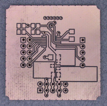
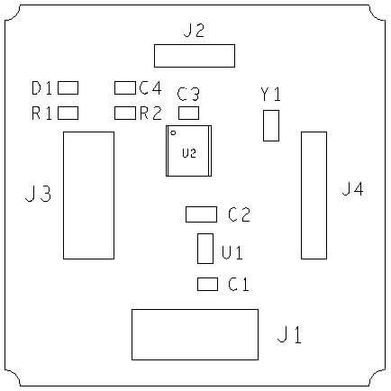
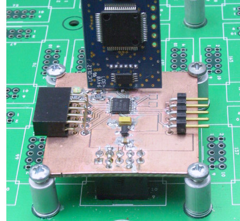
To view the signal we will need to connect the scope to P1.2.
We could do this with the scope probe or clip leads, but the
safest, most robust way is to use coax cables.
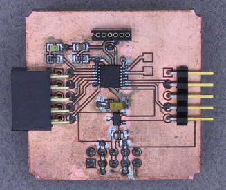
There should already be a BNC to SMB connector module on the breadboard.
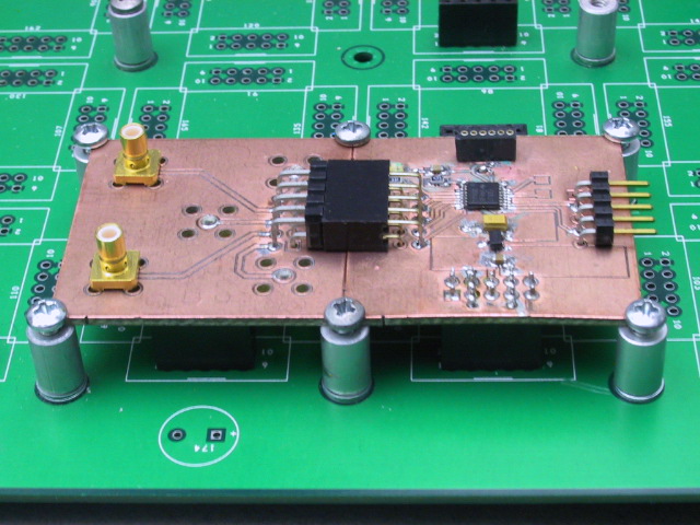
The module shown below provides a interface between J3 on the processor board
and a set of 5 SMB connectors, one for each of the signals on J3.
(We only need two of these signals, so only two of the SMB connectors have
been installed.)
(Click to enlarge)
Connect this module to the processor module, resulting in the
assembly shown below:
(Click to enlarge)
Use a BNC cable and an SMB cable to connect P1.2 to the scope.
|
Run your program. |
|
Using the same procedure as in the previous Part, compile, load, and run
your program.
If all goes well, the light should flash and a low frequency square wave should
appear on the scope.
|
Make the light flash faster. |
|
The low frequency of the signal makes it easy to see on the LED
but hard to observe on the scope.
To improve the latter at the expense of the former, modify your program
to increase the frequency of the signal to the point where it comfortable
to observe on the scope.
|
There are a variety of different A/D converter types in
the MSP430 family.
We have chosen the 2012 (rather than the 2011 or 2013) because it
contains a successive approximation converter, which is
faster and easier to use than the other choices.
| |
|
|
Add still more hardware. |
|
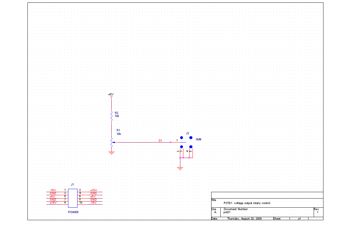
In order to test the A/D converter, we will need an analog signal source.
We could use the function generator, but a more useful source for
our current needs is a manually adjustable voltage.
The easiest way to get this is with a potentiometer acting as a
voltage divider for the Vcc supply voltage.
Fortunately, we have a module which does precisely that:
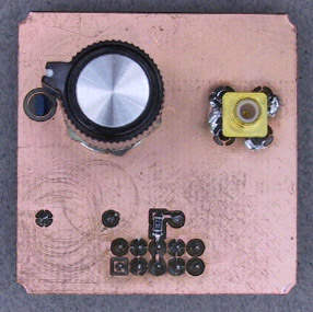
(Click to enlarge)
As circuits go, it's pretty simple:
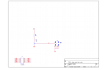
(Click to enlarge)
Note the 10 kΩ fixed resistor which limits the output voltage
range to 0-2.5 V, in order to match the range of the A/D converter.
|
Make the connections. |
|
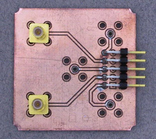
Place the potentiometer module in a convenient location and use a
coax jumper to connect its output to P1.4 (the lower-left SMB connector
on the connector module).
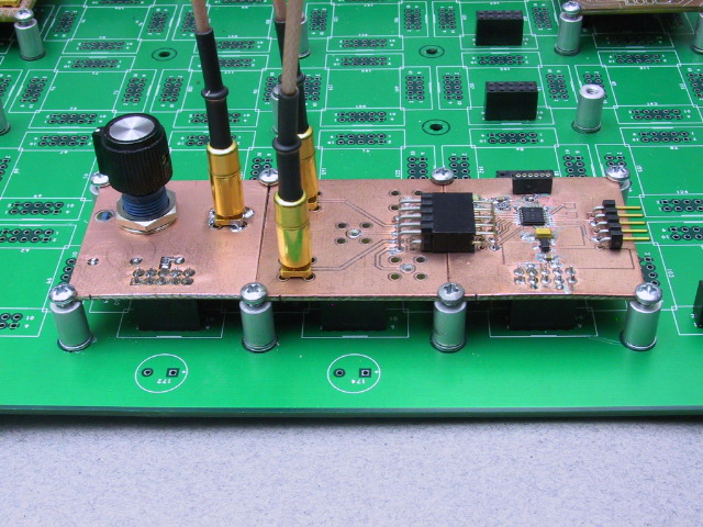
(Click to enlarge)
Since the potentiometer is connected via a coax cable, it doesn't
have to be directly adjacent to the connector module.
|
Download the A/D converter code. |
|
Programming the A/D converter is considerably more complicated than
programming the digital I/O pins, requiring 31 pages in the User's Guide
to describe it vs. 8 for digital I/O.
It's even more complicated than that, since the A/D converter interacts with
the Basic Clock Module (another 18 pages).
Although you should certainly read and understand those pages,
a faster way of getting the A/D up and running is to start with
some code that already works, and make changes until it works the way
you want it to.
Such a program, and another for use in the next Part,
are available in the
zip file for Exercise 2.
Download this file and unzip it into the directory you created in the
previous Part.
It will create a subdirectory named "lab2".
|
Build and run the program. |
|
Open the workspace file
lab2.eww
in the lab2 directory.
Select and build the
adc1
project.
This program reads the analog input on pin P1.4 and compares it to a
fixed threshold (1/2 full scale).
If it is greater, it turns on the LED, if less it turns it off.
Compile, load, and run the program and verify that it works as
intended.
|
Modify the program. |
|
Knowing when a physical variable (represented by the voltage on pin P1.4)
reaches a particular value is a potentially useful function in a design,
so this program might have some utility beyond simply testing the A/D converter.
It would have more utility if the threshold value could be changed.
Right now our only way of changing it is by editing and recompiling the
program.
Make the required modifications to set the threshold to a different level
(e.g. 1/4 full scale) and verify that your new program functions as
intended.
|
We will use the same hardware setup as we did in the previous part.
However, instead of turning the LED on and off, the signal produced by
the potentiometer will be used to control the duty cycle of the signal
on P1.2.
Since the MSP430 timer is almost as complicated as the A/D converter
(24 pages in the User's Guide),
we will once again make use of pre-written code.
| |
|
|
Select and build the pwm project. |
|
The code for this part is in the same zip file as that for the previous Part.
Simply select the
pwm2
project, build, and load.
|
Verify that it works. |
|
Set the potentiometer to mid-scale and start the program
If all is in order, you should see a square wave of about 50% duty cycle
on the scope.
Adjust the potentiometer and see how the waveform changes.
Characterize this behavior in terms of pulse frequency, relationship of duty cycle
to input voltage, etc.
|
Signal integrity. |
|
Increase the sweep rate on the scope until you can see the ringing on the
rising and falling edges of the PWM output signal.
Verify that it's caused by reflections by terminating the cable at the
scope using a BNC T-connector and a 50 Ω terminator.
Is this ringing significant?
|
Programming Challenge. |
|
Rather than modifying the code as in the previous two parts, this time you get
to completely (or at least substantially) rewrite it.
The details are in the
next
section, but basically your task is to replace the function of the timer
with software.
For instructions on how to start a new IAR project, see
Starting a new MSP430 project.
|