(Click to enlarge)
The other serial protocol we will look at in this exercise is I2C, which is a clever way of writing IIC, which in turn is short for Inter IC Communication. This is a protocol designed for efficient communication between microcontrollers and peripherals, or between several microcontrollers in a network. For details, see the I2C-bus Specification and User Manual.
For the asynchronous protocol in the previous section, all the components (PC and RS232 level converter) were already available. Unfortunately, this is not the case for I2C. This means we will have to build something to connect the MSP430 to before it can speak I2C.
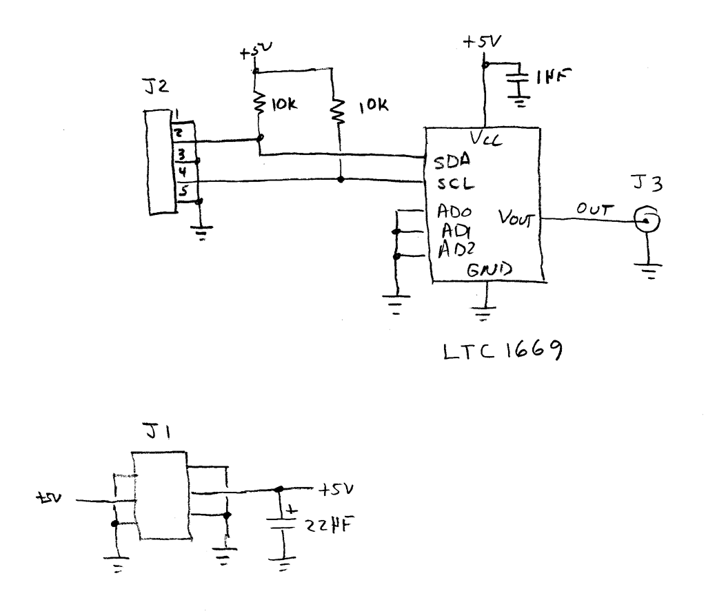
Our choice for this project is the LTC1669 10-Bit Rail-to-Rail Micropower DAC with I2C Interface. It's easy to use, it provides a D/A conversion function which is missing from the 2012 branch of the MSP430 family, and we have a bunch of them. The only problem is that they are in a bag, not on a board. And unlike the previous two exercises, there aren't any blank boards available to solder them onto. We are going to have to design and fabricate the required PCB from scratch.
PC board layout has the reputation of being really hard. This is not strictly true. What's true is that it's really hard to learn. There are a number of reasons for this. The layout process itself is fairly challenging, but it has been made more difficult by the software which is used to perform it.
In spite of its up to date visual appearance, much of this software embodies an architecture which reflects a much more primative environment than is the norm today, and was written by the people who were going to use it, rather than by people trained in software design. Such software is easy for its authors to use, but not necessarily easy to learn by someone who wasn't involved in writing it.
The most powerful software is often the worst in this regard, not just because more power usually entails more complexity, but because this power has grafted piecemeal onto the original product over a long period of time.
The good news is that there are a number of modern, relatively easy to use PC layout packages available. Some of these are even available for free. The bad news is that the package we have chosen to feature in this course is not one of those. The reason for this choice is that we will eventually want to utilize the power that this package offers. Fortunately, although this package has a very steep learning curve, once learned it is relatively easy to use, often more so than packages which are easier to learn. Another bit of good news is that it is possible to bypass many sections of the learning curve by starting with a pre-configured design template, rather than from scratch. This is the approach that we will take. Rather than start at the front of the documentation and work our way through, we will take a short cut which allows us to start laying out boards for our 332 breadboard system fairly quickly. We will deal with the features that we skipped over one at a time, as need for them arises.
Our streamlined painfree approach is embodied in our own, custom tutorial. Since the example used in this tutorial is exactly the circuit we want to build, this part of this week's exercise should be smooth, though perhaps lengthy.
If you wish to use a different package, feel free to do so. However, its output must be compatible with that of the Cadence package.