ELEC 332

In the Lab

Part 1: Breadboarding the Transistor Buffer


Construct the transistor buffer circuit.

Using an appropriate prototyping technique, build the circuit shown in the previous section, with a 1 kΩ collector resistor and a 10 kΩ base resistor. If you're very careful, you can build the circuit on a 241 breadboard. However a better approach would be to use dead bug construction using one of the leftover scraps of PCB material. If you want the ultimate in high performance construction, you can use surface mount components. We have the surface mount version of the 2N3904 (called MMBT3904) available.

Whatever technique you choose, here are A few things to remember

  • In the actual circuit there will be a bypass capacitor on the Vcc supply line. Be sure to include one in your breadboard.
  • In the actual circuit, the input to the buffer will be driven by a low impedance source with a very short connection. If you use the function generator to drive your breadboard circuit, it will be at the other end of a long piece of coax. You will need to properly terminate the cable to avoid reflections.
  • Make all of your measurements with the 10x probe.


Measure the response to a pulse input.

Set up the function generator to produce a 500 kHz square wave. Adjust the amplitude and offset so that the low value is 0 V and the high value is 3.3 V when connected to your circuit (i.e. when properly terminated). Sketch the output waveform. Measure the rise and fall times and the propagation delay for both rising and falling outputs.

Add a capacitor.

Place a 100 pF capacitor in parallel with RB and repeat the measurements of the previous step.

Try different values of capacitor.

Repeat the previous step with a variety of different capacitor values between 10 and 200 pF. What is the "best" value?

Part 2: Time Domain Simulations

For a circuit this simple, exploring the design via a breadboard should be fairly quick, assuming you have a pile of capacitors handy. However, for more elaborate circuits or for studying the interaction of several different components using simulation rather than actual construction could save time.

Rather than introduce a more elaborate circuit at this point, we'll use the one from the previous part and see how well the Pspice simulation matches our measurements.


Start Orcad Capture.

The front end to Pspice is the same program we have used for the schematic capture phase of PCB layout, so we already know most of what we need to know.

Enter or load the schematic.

If you want, you can create a new project and enter the schematic yourself. Just remember to check the "Analog or Mixed A/D" box rather than "Schematic". You can place and connect components just as you did for PCB layout. The components will come from a different set of libraries, so you can't reuse PCB layout schematics.

However, as with PCB layout, there are a number of unobvious options that need to be set, so it's best to start with a working project and modify it rather than start from scratch.

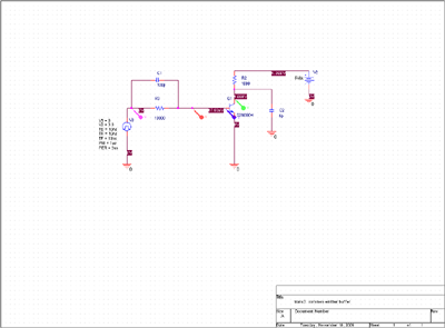
Extract the lab9 directory from this week's zip file. Select Open->Project ... from the File menu, navigate to the lab9 directory that you extracted from the zip file, and open the trans3.opj file. You should see the following schematic:


(Click to enlarge)

You should also see an addition to the toolbar:

These buttons control the simulation process and the placement of measurement points (probes).

Run the simulation.

Press the Run button (). This will start the simulation, and after some clicking and whirring the Pspice display window will pop up. This will show each voltage and current in the circuit which has been marked with a probe. The color of the trace will correspond to the color of the probe.
Observe the output.

How well does the simulation display correspond with what you observed in the actual circuit?

Remove the capacitor.

Remove the capacitor which is in parallel with the base resistor (C1) and rerun the simulation. How well does the result match the actual circuit?

Try different values of capacitor.

Run the simulation with a variety of different capacitor values between 10 and 200 pF. Is the best value the same as for the actual circuit?

Part 3: Frequency Domain Simulation

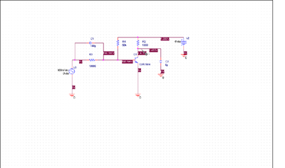
Spice can also be used to perform frequency domain simulation. There are two ways of doing this. One is to take the Fourier transform of the time domain transient response. (Try pushing the FFT button in the Pspice display window.) The other is to measure the steady state response to a sine wave of varying frequency (as in 241 lab). The latter measurement is performed using a linearized, small-signal model of the circuit, so we can't use it to see what our level shifter is doing in the frequency domain. However, we can use it to see what our level shifter would do in the frequency domain if it were biased to operate in the linear region of its transfer characteristic. We can do this by adding a single resistor, as shown in the circuit below.


(Click to enlarge)
We also need to replace the pulse generating voltage source with a tuneable sine wave voltage source, and change a few of the options to enable the AC analysis. These have all been done in the trans4.opj file which is included in this week's zip file.


Load the new Pspice project file.

Navigate to the directory where you extracted the lab9.zip file and open the trans4.opj project file.

Run the simulation.

When the Pspice display window pops up, it will display the frequency response rather than the time response. You can get a log-log plot by pushing the logarithmic Y-axis button.

Remove the capacitor.

Remove C1 and rerun the simulation. The rather poor high frequency response is not a result of base charge storage (which happens when the transistor saturates), but of junction capacitances, another thing we didn't talk about in 242.

Try different values of capacitor.

Run the simulation with a variety of different capacitor values between 10 and 200 pF. Which value gives the best frequency response?

Build and measure the circuit (optional).

Although it would be easy to modify your breadboard circuit to match the one we've been simulating, performing the frequency response measurements would be tedious (remember 241). If you have a burning desire to verify that the simulation is valid, by all means do so. If not, move on to the next step.

Note: if you do decide to build the circuit, you will almost certainly have to change the value of the bias resistor (R4). Its value depends strongly on the beta of the transistor, which varies greatly from one device to another.