(Click to enlarge)
(Click to enlarge)
| 1. | Tools->Padstack->Modify Library Padstack | |||
|---|---|---|---|---|
| You aren't actually going to modify the library padstack, just use it as a starting point. | ||||
| 2. | Select a suitable existing padstack. | |||
| Start with a pad as close as possible to the one you want to define. For most pads, the size and shape can be determined from the name. For example, "Pad50cir30d" is a circular pad 50 mils in diameter with a 30 mil drill hole, "Smd30rec14" is a rectangular surface mount pad (top surface only, no hole) 30 mils wide and 14 mils tall, etc. | ||||
| 3. | Create a new padstack file. | |||
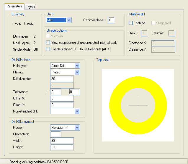
| 4. | Set the drill size. | |||
| (Skip this step for a surface mount pad.) In the "Parameters" tab, set the Drill diameter to the desired hole size. |
(Click to enlarge) | |||
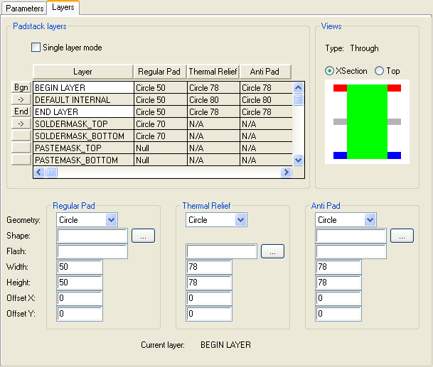
| 5. | Set the pad dimensions. | |||
| Select the "Layers" tab and set the shape and dimensions of your pad in the Regular Pad area for the BEGIN LAYER, END LAYER, and DEFAULT INTERNAL. Set the dimensions of the solder masks, thermal relief, and anti-pad to be larger by an amount consistent with your design rules. If you can't find the appropriate information, change them by the same amount that you changed the original dimensions of the pad itself. |
(Click to enlarge) | |||
| 6. | Save the new pad. | |||
| If you didn't do a Save As earlier, be sure to save the pad in your own library. Don't overwrite the original. |
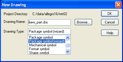
| 1. | Start a new drawing. | |||
|---|---|---|---|---|
| Select New ... from the File menu. Browse to your symbol directory (<home>/pcb/symbols) and enter the name of your part. Select Package symbol (wizard) as the drawing type. Clik OK. |
(Click to enlarge) | |||
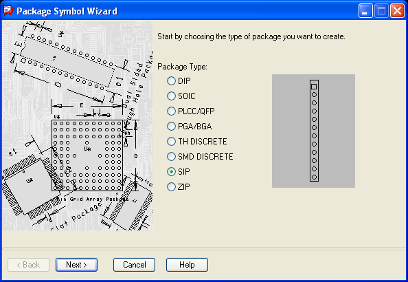
| 2. | Select package type. | |||
| Our header is a single row of pins, so we will choose SIP. |
(Click to enlarge) | |||
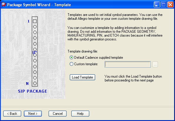
| 3. | Select package template. | |||
| Just accept the default here. However, before clicking Next you must click Load Template. |
(Click to enlarge) | |||
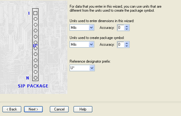
| 4. | Set General Parameters. | |||
| For out connector we can accept the defaults here. If defining a package with metric dimensions, choose Millimeter for Units used to enter dimensions in this wizard. |
(Click to enlarge) | |||
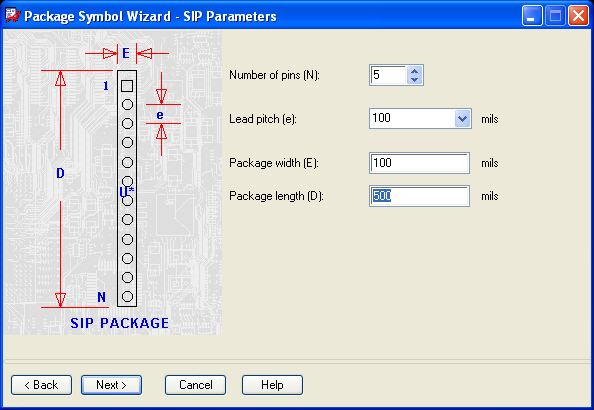
| 5. | Fill out SIP Parameters. | |||
| Enter the number of pins, pin spacing, and package outline dimensions. Click Next to go to the next step. |
(Click to enlarge) | |||
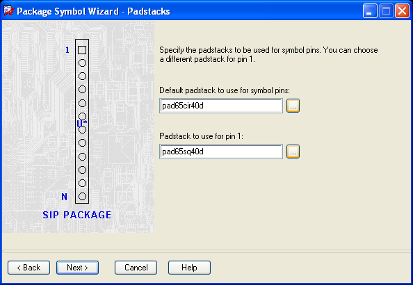
| 6. | Enter the padstack names. | |||
If the required padstack is not already in the library, define it as
described above in
Creating a Padstack
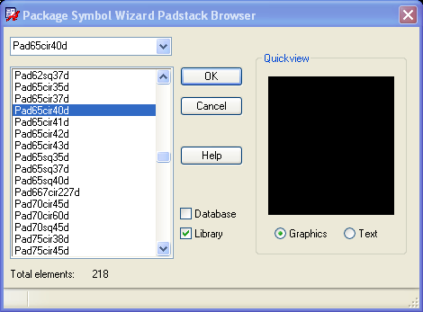
Once the desired padstack is properly defined, click on the
( )Browse
button and select it from the
Padstack Browser
dialog. )Browse
button and select it from the
Padstack Browser
dialog.
|
(Click to enlarge) | |||
| Thru-hole pads have names like PAD65CIR40D or PAD65SQ40D. The first number is the diameter of the pad (in mils) and the second is the diameter of the hole. "CIR" indicates a round pad and "SQ" a square one. It is often useful to indicate Pin 1 by giving it a different shape from the other pads, so we will choose a square pad for it, and round ones for the other pins. |
(Click to enlarge) | |||
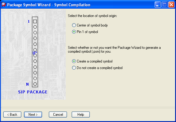
| 7. | Symbol Compilation | |||
| This is the point where the wizard actually builds the footprint. You have two choices to make. You should always accept the default on the second, to create a compiled symbol, as that is the whole point of this exercise. The first, where to put the symbol origin, is often a matter of personal preference. However, in this case our connector has to be placed at a precise location on the board, so placing the origin on Pin 1 is the best choice. |
(Click to enlarge) | |||
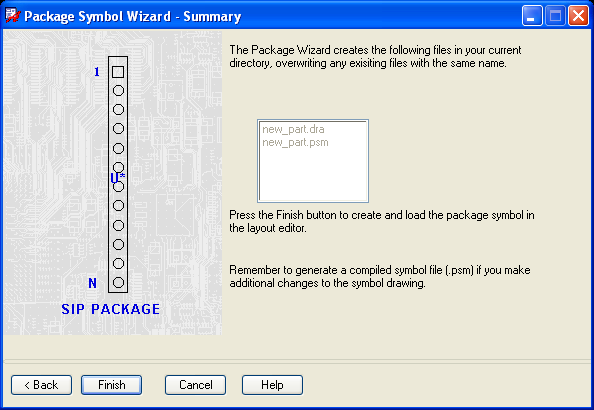
| 8. | Summary | |||
| This step tells us that the wizard has completed its work. Click Finish to see the results. |
(Click to enlarge) | |||
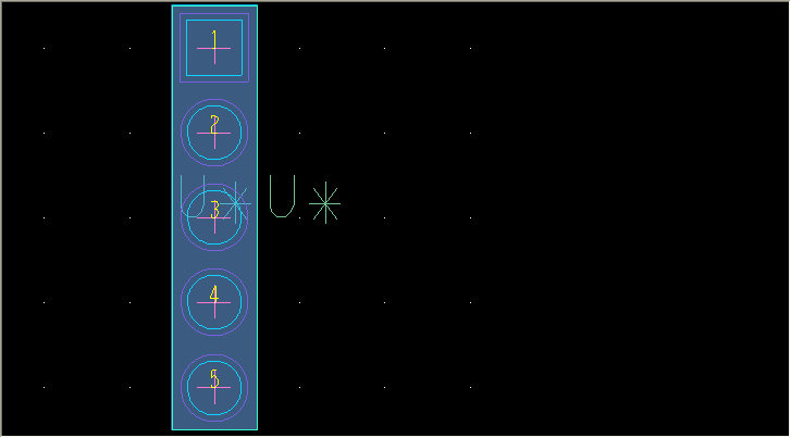
| 9. | Edit | |||
| When the wizard is finished, it returns us to Allegro to view, and possibly edit, the footprint. The assignment of colors to layers is different from that in our standard .brd file, so things won't look quite right. At this point you can make any necessary additions, deletions, or modifications. There's nothing we really have to do to this footprint, but it would be easier to use if we moved the package label (U*) which is located in the middle of the footprint to another location, e.g. on top of the other label. |
(Click to enlarge) | |||
| 10. | Save | |||
| If you made any changes in the previous step, select Save from the File menu to save the edited footprint. |