(Click to enlarge)
PC layout is one of many steps in the design process. As such it accepts inputs from previous steps, as well as from external sources, processes them, and produces outputs which will be used in subsequent steps. Before beginning this step it is necessary to gather these inputs and organize them into an efficient structure.
| 1. | Your circuit diagram. | |||
|---|---|---|---|---|
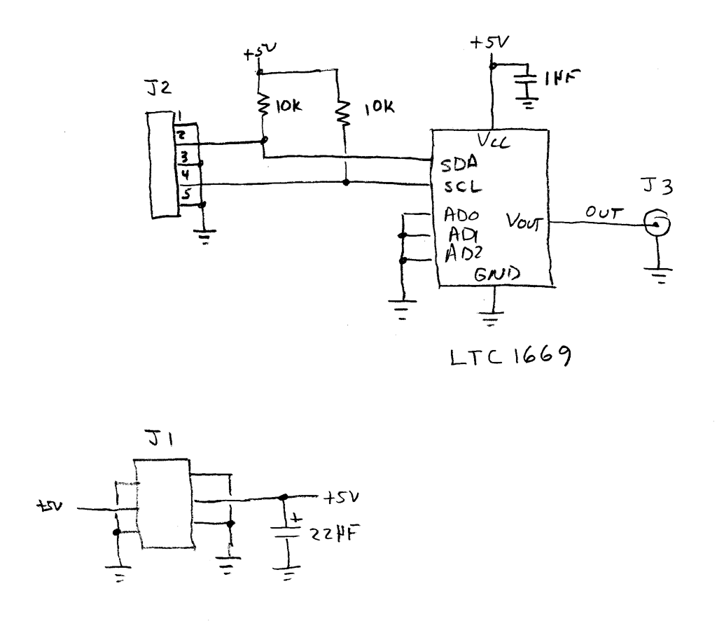
| Once you become proficient in using the design tools, you should be able to create your initial schematic directly in the schematic capture program. At first, it's best to have a hand-drawn diagram to work from. We'll be using the circuit sketch from Exercise 3. |
(Click to enlarge) | |||
| 2. | Data sheets for all components. | |||
| For every component in your design you will need to know the pin assignments (function vs. pin number) and the physical dimensions. Resistors and capacitors are pretty simple (only two pins) and well standardized (0805 tells you everything you need to know about the size). For every other component you should have available the manufacturer's data sheet, catalog entry, outline drawing, etc. Try to find documents with suggested PCB pad/hole patterns. | ||||
| 1. | Download and unzip the startup directory. | ||
|---|---|---|---|
|
The zip file
lab3.zip
provides a directory structure
and set of files which provides all of the necessary files
in appropriate locations to begin work on
this week's board.
There are two directories in this zip file:
lab3
contains the MSP430 programs used in this weeks lab exercises and
pcb
contains a skeleton directory for pcb layout.
We will refer to the location where you have placed the contents of the zipfile
as <home>,
so that <home>/pcb will be your copy of the layout directory.
As the semester progresses, this directory will be expanded and updated to accommodate the various boards we will be building. Since this will become a valuable resourse for you success in this course, you should keep it in a safe place. Recommended locations are a USB flash drive which you keep with you at all times or your "U" drive from ADRICE. In particular, don't keep it on one (or more) of the ELEC332 lab PCs. | |||
| 2. | Create a directory for the new design. | ||
| Since this directory will eventually contain a number of different designs, we will keep each one in a separate directory. We'll begin to put stuff in this directory in the next phase of the tutorial. However, now would be a good time to build a home for this stuff. Create a directory named "adc" in the <home>/pcb directory. |