
(Click to enlarge)

(Click to enlarge)

(Click to enlarge)

(Click to enlarge)
 set the
Import directory:
field to <home>/pcb/adc/allegro,
then click the
Import cadence
button
set the
Import directory:
field to <home>/pcb/adc/allegro,
then click the
Import cadence
button

(Click to enlarge)
One reason that PCB layout software has such a steep learning curve is that before anything useful can be done, a very large number of options must be set and a large number of auxilary files must be in place. Figuring out from scratch what these are and what values and contents they should have requires wading through literally reams (if it were on paper) of documentation. To save you having to do that (at least at this point) we have assembled an initial environment containing a set of files which are ready to go.
| 1. | Copy Board Template File to Design Directory | |||
|---|---|---|---|---|
| Copy the files "BRD1x1.brd" and "nc_tools.txt" from <home>/pcb/boards into <home>/pcb/adc. Rename the copy of BRD1x1.brd to "adc.brd". | ||||
| 2. | Start Allegro PCB Editor. | |||
|
(Click to enlarge) | ||||
| Once again there's a space consuming text window (the command window) at the bottom of the screen. However, we will need it this time around, so we'll leave it there. |
(Click to enlarge) | |||
| 3. | Load the blank board file. | |||
| File->Open... to bring up the dialog box. Make sure the Files of type: field is set to "Board," then select "adc.brd" and click Open. |
(Click to enlarge) | |||
| You should see the blank board displayed in the main window. In addition to the outline and pre-positioned power connector, this board has most of the essential options set to appropriate values for our project. |
(Click to enlarge) | |||
| 4. | Import the netlist. | |||
|
File->Import->Logic...
Using the browse button (
set the
Import directory:
field to <home>/pcb/adc/allegro,
then click the
Import cadence
button
|
(Click to enlarge) | |||
| If all goes well, you'll get the message "netrev completed successfully" in the command window. If all doesn't go well messages describing the problem will appear in the command window. |
| 1. | Run quickplace. | |||
|---|---|---|---|---|
| From the Place menu, select Quickplace.... The quickplace dialog will appear. Accept the defaults and click Place. |

(Click to enlarge) | |||
| All of the components in your design will be deposited directly above the board outline. Click OK on the quickplace dialog to make it go away. |

(Click to enlarge) | |||
| The green spots are the pads (green indicates copper on the top of the board, red is copper on the bottom). The pink rectangles are the part outlines. The pale yellow and blue lines are the rat's nest which indicates where connections should be make, but haven't been. | ||||
| 2. | Start Edit Move mode. | |||
Unlike modern graphic editing programs, Allegro is highly modal.
The current mode is indicated by the word in the lower left corner of the
window.
When nothing is happening, this will say "Idle."
To move an object, you don't just click on it and drag, you select
move
mode,
then you set a list of things that are eligable for selection,
then
you click on the object to select it.
At this point you can move it to the desired location.
Once it's there you
click again
it to fix it in its new location.
To enter move mode, click on the move button
( )
or select Edit->Move from the menu.
At this point the mode word in the lower left corner will change to "move." )
or select Edit->Move from the menu.
At this point the mode word in the lower left corner will change to "move."
| ||||
| 3. | Set the find filter. | |||
| Allegro supports a large collection of object types and subtypes. In some cases two objects of different types may be in the same location. To enable selecting objects of the desired type or to avoid selecting objects of an undesired type, Allegro has a find filter. This is a list of the types of object which a selection operation will recognize. The selection filter is controlled by the find panel, which is normally hidden. To make it visible, click on the vertical Find tab on the right hand edge of the screen. This will bring up the find panel. For the time being we'll leave it as is (all objects selectable). |

(Click to enlarge) | |||
| 4. | Move U1. | |||
| Move the cursor over the symbol for U1. When it is selectable, the symbol will be highlighted and a rectangle containing identifying information will appear. |

(Click to enlarge) | |||
| Left click when the symbol is selectable. The origin of the symbol (pin 1 in this case) is now attached to the cursor and may be moved. Notice that the rat's nest lines remain attached and move with the symbol. |
(Click to enlarge) | |||
| Position U1 at the approximate center of the board and left click again. It will remain in this position. | ||||
| 5. | Place connector J2 | |||
| In order to mate with the corresponding connector on the CPU module, J2 must be in the correct location on the board (pin 1 at (280,950)). Place the cursor over the symbol for J2 and left click to select it. On the keyboard type "x 280 950" and hit <Return>. The symbol will be placed with its origin (again pin 1) at the specified location. | ||||
| 6. | Place remaining components | |||
| Position the remaining components at appropriate locations on the board. The rat's nest lines show where connections must be made, so your placement should minimize their length and number of crossovers. Since we will be using a ground plane, don't worry too much about ground connections. They can be made directly to the other side of the board using vias. | ||||
| Some components may be easier to route if they are rotated. To rotate a component while in move mode, right click and select Rotate while the component is selected. This will attach a handle (the white line in the screenshot) by which the component may be rotated. Move the cursor around until the desired orientation is achieved and left click. This will end the rotation and return to move mode with the component still selected. Move it to the desired location and left click again to place it. |

(Click to enlarge) | |||
| When you have placed all of the components, right click and select Done. This will exit move mode and return to idle. Your layout might look something like this: |

(Click to enlarge) | |||
| 7. | Clean up component labels. | |||
| The labels for the various components, "C1", "J1", etc. are positioned inconsistently. Not only does this look untidy, but it can make it possible to mistake the location of a component when assembling the board. We can fix this by moving and rotating the labels with the move command. To allow us to select only the label, and not the entire component, bring up the find filter panel, click AllOff and then check only the Text box. |

(Click to enlarge) | |||
| When moving labels, a white line is drawn between the label and the component to which it belongs. This makes it easy to associate a label with the correct component. |

(Click to enlarge) | |||
| 1. | Zoom to fit. | |||
|---|---|---|---|---|
One conventional aspect of Allegro's navigation are the zoom buttons.
Use the
Zoom Fit
button
( )
to fit the board to the window size. )
to fit the board to the window size.
|

(Click to enlarge) | |||
| 2. | Zoom in and pan. | |||
| We will want things bigger than this for routing, so click on the Zoom In button. Things are now bigger, but most of them are off the screen. How to fix this without scroll bars? If you have a mouse with a center button, hold it down and move to the left. This causes the window to move to the left, so that the contents appear to move to the right. This is the opposite of most graphics programs where panning grabs the underlying sheet of paper and moves it with, rather than against, the cursor. | ||||
| If you don't have a three button mouse, you can use the arrow keys on the keyboard to scroll the window in steps. Or you can use the Worldview window in the lower right of the screen. This represents the main window when zoomed to fit: the yellow square is the outline of our board. To zoom into an area of the board, left click and drag a rectangle around the area of interest (the rectangle will automatically be shaped to the aspect ratio of the main window). The screen shot shows the view zoomed into the lower right quarter of the board. |

(Click to enlarge) | |||
| 1. | Pin down the Options panel. | |||
|---|---|---|---|---|
During routing we will be accessing the
Options
panel frequently.
It will be more convenient if it is displayed continuously, rather than
having to pop it up every time we need it.
To do this, move the cursor over the
Options
tab on the right hand edge, then move to the pushpin button
( )
and click. )
and click.
| ||||
| 2. | Enter connect mode. | |||
Click the
Add Connect
button
( )
or select Route->Connect from the menu.
The mode field in the lower left corner will change to
add connect
and the
Options
panel now contains the things we need to control during routing.
The ones we will be most concerned with are the active routing layer
(Act), the alternate routing layer (Alt) and the
line width. The defaults should be adequate for the others. )
or select Route->Connect from the menu.
The mode field in the lower left corner will change to
add connect
and the
Options
panel now contains the things we need to control during routing.
The ones we will be most concerned with are the active routing layer
(Act), the alternate routing layer (Alt) and the
line width. The defaults should be adequate for the others.
|

(Click to enlarge) | |||
| 3. | Route the first trace. | |||
| We will start by routing the SDA signal from J2-2 to U1-1. Zoom and pan so that J2 and U1 fill the main window. Be sure that Top is selected as the active layer. Position the cursor over pin J2-2 and left click. The pad, the rat's nest, and all other pads connected to this net will be highlighted. |

(Click to enlarge) | |||
| Move the cursor away from the pad. A thick green line will follow it around, with the other end connected to the pad. |

(Click to enlarge) | |||
| Move the cursor to the lower pad of R1 and click again. This completes the connection. |

(Click to enlarge) | |||
| Repeat this process, starting on pin 1 of U1 and connecting again to the lower pad of R1. This completes the first net. |

(Click to enlarge) | |||
| 4. | Connect the DAC output. | |||
| Pan the window so that J3-1 and U1-8 are both visible. Return to add connect mode if you have left it. Insure that Top is selected as the active layer and Bottom is the alternate layer. Click on the pad for U1-8 and move the cursor until it is directly beneath J3-1 and two grid spaces below the outline of J3. |

(Click to enlarge) | |||
| 5. | Add a via. | |||
| Since the center pin of J3 is not accessable from the top of the board, we can only solder it on the bottom. This means we will have to move our trace from the top of the board (the only place it can connect to U1-8) to the bottom (the only place it can connect to J3-1). We will do this with a via. Since the portion of this trace on the bottom of the board will interrupt the ground plane, something we wish to avoid as much as possible, we want to place the via as close as possible to J3-1. Since it must be soldered from both sides, it must be outside the boundary of J3. | ||||
| With the cursor still positioned as in the previous step, left click to anchor the end of the trace. Then right click and select Add via. |

(Click to enlarge) | |||
| Move the cursor to J3-1. Note that the trace is now red, indicating that it is on the bottom of the board. Left click to complete the connection. |

(Click to enlarge) | |||
| 6. | Route power lines. | |||
| Since this chip uses very little power supply current (about 0.1 mA) we could use the default 12 mil trace width to route the power lines. However, it's good design practice to make power traces as wide as possible. We'll compromise and make them twice as wide as the signal traces, i.e. 25 mils. Zoom and pan so that J1, C1, and C2 are all visible. Enter add connect mode and set the active layer to Top. Click in the Line width: field, type "25" and hit <Enter>. Click on J1-6 to start the trace, move to the left-hand pad of C2 and click again to end it. Similarly, connect the left-hand pad of C2 to the lower pad of C1 and the lower pad of R2. Connect J1-5 to J1-6. We can't connect a 25 mil trace to a pad of U1, so change the line width back to 12 mils and connect U1-5 to the lower pad of C1. It may be helpful to left click at various intermediate points to control the path of the trace. If you make a mistake, right-click and select Oops. |

(Click to enlarge) | |||
| 7. | Add vias to ground. | |||
| The ground pins of J2 and J3 are accessable from the bottom of the board and can be soldered directly to the ground plane. All other ground connections, including those for J1 must be connected to the ground plane with vias which are accessable for soldering from both sides of the board. | ||||
| Enter add connect mode, select the top layer as active and bottom as alternate layer. Set the line width to 25 mils. Click on J1-4, move straight up until the cursor is two grid spacings above the border of J1, and click again. Right click and select Add Via, then right click again and select Done. This via is currently connected to nothing on the back side of the board, but when we add the ground plane, Allegro is smart enough to do the right thing with it. Note that when you placed the via above J1-4, Allegro changed the active layer to the bottom, in anticipation of the trace continuing there. If you want to continue wiring on the top (which we will in the next step) you will have to switch it back before proceeding. |

(Click to enlarge) | |||
| Do the same thing with with J1-8, then connect J1-3 to J1-4 and J1-7 to J1-8. Connect the via above J18 to the right-hand pad of C2. |

(Click to enlarge) | |||
| 8. | Complete the remaining connections ... | |||
| with 12 mil traces and vias to ground where necessary. |

(Click to enlarge) | |||
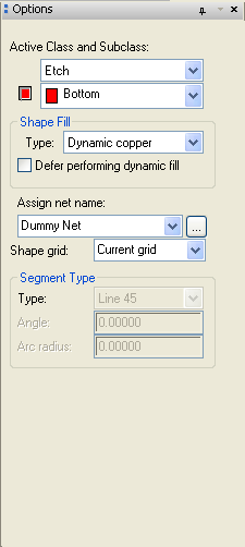
| 1. | Start the add rectangle tool. | |||
|---|---|---|---|---|
Click on the
Shape Add Rect
button
( ).
In the options panel, set the
Class
to "Etch"
and the
Subclass
to "Bottom." ).
In the options panel, set the
Class
to "Etch"
and the
Subclass
to "Bottom."
|
(Click to enlarge) | |||
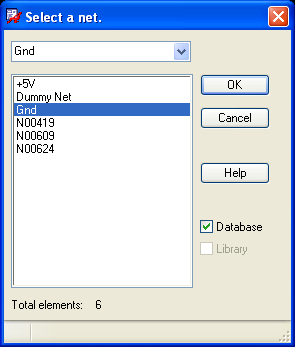
| In the Assign net name: field, click on the browse box and select "Gnd" |
(Click to enlarge) | |||
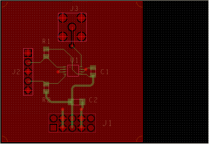
| Zoom to fit to bring the entire board into the window. Left click in the upper left corner of the board, then move to the lower right and click again. You have just created the ground plane. |
(Click to enlarge) |
| 1. | Set artwork parameters. | |||
|---|---|---|---|---|
Click on the
Artwork
button
( )
or select
Artwork...
from the
Manufacture
menu.
This will bring up the
Artwork Control Form.
Ignore the warning message.
On the
General Parameters
tab select "Gerber RS274X"
as the
Device type.
Ignore the warning messages.
The defaults are satisfactory for the other parameters. )
or select
Artwork...
from the
Manufacture
menu.
This will bring up the
Artwork Control Form.
Ignore the warning message.
On the
General Parameters
tab select "Gerber RS274X"
as the
Device type.
Ignore the warning messages.
The defaults are satisfactory for the other parameters.
|

(Click to enlarge) | |||
| Click on the Film Control tab. Check the BOTTOM and TOP boxes in the Available films list. |

(Click to enlarge) | |||
| 2. | Generate apertures. | |||
| Click on the Apertures... button. On the Edit Aperture Wheels dialog, click the Edit... button. |

(Click to enlarge) | |||
| On the Edit Aperture Stations dialog, click on Auto-> and select Without rotation. Click OK on the Edit Aperture Stations dialog, then click OK on the Edit Aperture Wheels dialog. |

(Click to enlarge) | |||
| 3. | Generate artwork files. | |||
| Click Generate Artwork on the Artwork Control Form. Examine the resulting report for errors. There may be several warnings, but these can generally be ignored. Close the Artwork Control Form. | ||||
| 4. | Generate drill tape. | |||
| Select Manufacture -> NC -> NC Drill... from the menu bar. Select Increasing for Tool sequence. Check the Auto tool select box and uncheck Repeat codes. Click on the Drill button. If all is well, you will get a message to the effect that "NC Drill completed successfully." Close the NC Drill window. |

(Click to enlarge) | |||
| 5. | Close Allegro. | |||
| Save your design and close the Allegro PCB Editor program. | ||||
| 6. | Gather files for fabrication. | |||
| The manufacturing data for your board is contained in three files in the <home>/pcb/adc directory: BOTTOM.art, TOP.art, and adc-1-2.drl. Collect these into a .zip file and submit them for fabrication. | ||||