(Click to enlarge)
(Click to enlarge)
(Click to enlarge)
(Click to enlarge)
| 1. | Start Orcad Capture | |||
|---|---|---|---|---|
| Depending on which version of the Cadence software you have, this may be named Design Entry CIS, OrCad Capture CIS, or simply OrCad Capture. | ||||
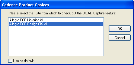
| 2. | Select Allegro PCB Design option | |||
| Before the program appears you will be asked which product option you want to use. Select "Allegro PCB Design CIS XL" then click OK. |
(Click to enlarge) | |||
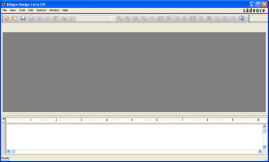
| 3. | Clean up the window. | |||
| The long thin panel at the bottom of the window is the session log. It's not very useful and it takes up valuable screen space. To make it go away, click the little box with the "x" in it in its upper left corner. |
(Click to enlarge) | |||
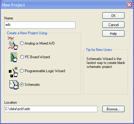
| 4. | Select File->New->Project from the menu. | |||
| You will get a dialog box like this. In the Location box, browse to the directory "<home>/pcb/adc" that you created previously. In the Name field, enter "adc". Select "Schematic" under Create a New Project Using. Finally, click OK. |
(Click to enlarge) | |||
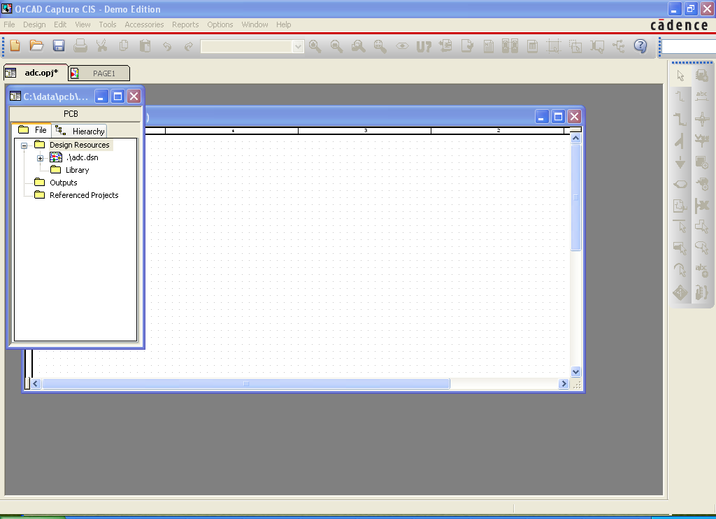
| You should have an empty schematic page and a project window, like this: |
(Click to enlarge) | |||
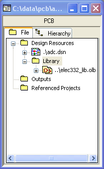
| 1. | Add the ELEC 332 library. | |||
|---|---|---|---|---|
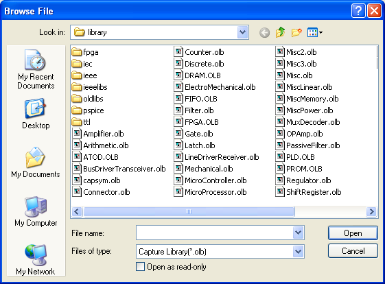
| Right click on the "Library" folder icon in the project window. Select "Add File". Browse to <home>/pcb and select ELEC332_lib.olb. |
(Click to enlarge) | |||
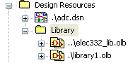
| 2. | Create a custom library. | |||
| Select File->New->Library from the menu bar. A new library named "./library1.olb" will appear. |
| |||
| Right click on this icon and select Save As.... Browse to the <home>/pcb directory and name the file "lab3.olb", then click Save. |
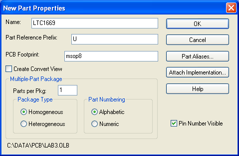
| 1. | Start a new part. | |||
|---|---|---|---|---|
| Right click on the "lab3.olb" icon and select "New Part." Enter "LTC1669" for Name and "msop8" for PCB Footprint. Click OK. |
(Click to enlarge) | |||
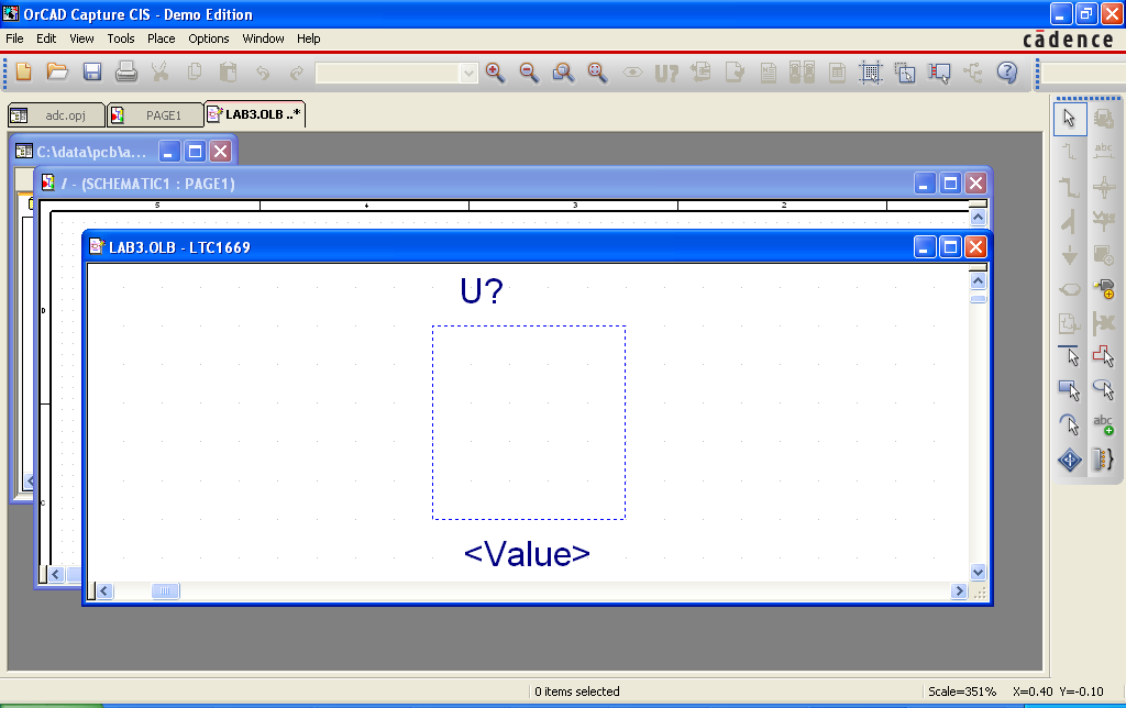
| A new window appears labeled "LAB3.OLB - LTC1669." This is where we will draw the symbol for the part. The dotted rectangle is the boundary of the part body (we can resize this if necessary). The "U?" label at the top is the placeholder for the part number and the "<Value>" label at the bottom is where the value (in our case the part number) will go. |
(Click to enlarge) | |||
| Notice the toolbar on the right-hand edge of the main window. Some of the tools are now active, while others are still greyed-out. The active tools are the ones we will use to draw the part. |
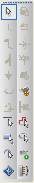
(Click to enlarge) | |||
| 2. | Place the pins of the part. | |||
| Refer to the data sheet for the LTC1669 for the pin assignments. | ||||
Click on the "Place pin" button
( )
in the right hand toolbar.
This will bring up the Place Pin
dialog box> )
in the right hand toolbar.
This will bring up the Place Pin
dialog box>
|
(Click to enlarge) | |||
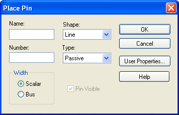
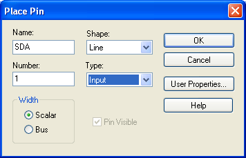
| We could arrange the pins in logical groupings as in the circuit sketch, or we could simply lay them out in numerical order as in the package drawing in the data sheet. By coincidence, it turns out that the default size of the outline in Capture is exactly the right size for the latter, so that's what we will do. For the LTC1669, Pin 1 is SDA. | ||||
| Enter "SDA" in the Name: field and "1" in the Number: field. Stick with "Line" for the Shape:. When in doubt, leave the Type: field set to "Passive." Since SDA is in fact an input, it is safe to choose this value for this pin. When you set the type to "Power" the Pin Visible field becomes active, and the default value is for the pin to be invisible. This is useful for basic gates or other simple parts where power pins would clutter up the drawing, but in general, invisible pins are a bad idea. If you set the "Gnd" and "Vcc" pin types to "Power," be sure to check the Pin Visible box. |
(Click to enlarge) | |||
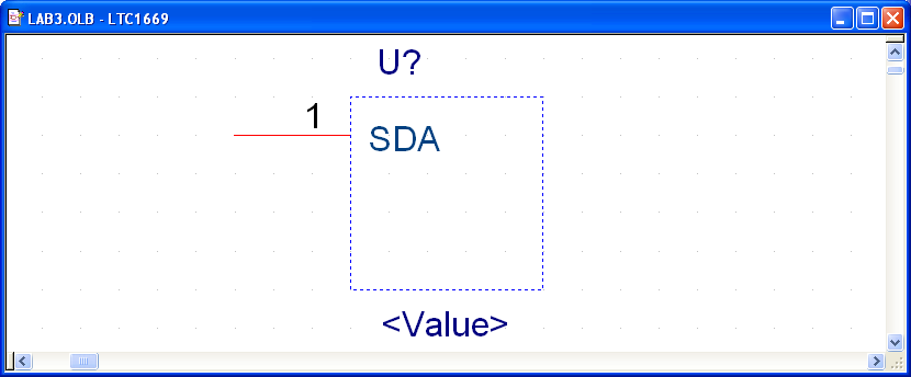
| Click OK. A line will appear, one end of which is stuck to the package outline, the other following the cursor around. This is the new pin. Place the cursor one grid step below the upper left corner of the package outline and click left. The pin will be deposited at this location. |
(Click to enlarge) | |||
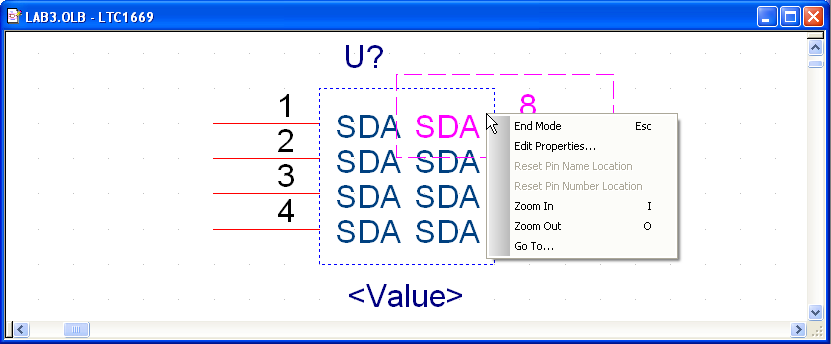
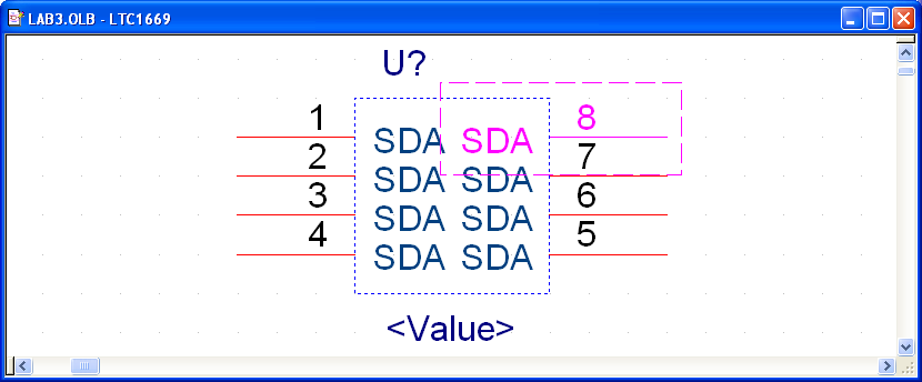
| When the first pin is placed, a new one will appear to follow the cursor around. If you place this one, it will be pin number 2 with the same name. If the pin name ended in a number (e.g. D1), that number would also be incremented, so this is a fast way to place consecutive bus pins. However, our pins are not so named, so manual intervention is required. There are two ways to do this. One is to place all of the pins, with the correct numbers but incorrect names, then go back and fix the names. The other is to bring up the Place Pin dialog for each pin. The former is a bit faster, so that's what we'll use. | ||||
| Once all the pins have been placed, right click and select End Mode. |
(Click to enlarge) | |||
| Now go back and edit pins 2-8. Left double-click over each pin to bring up the Place Pin dialog, change the name (and type if necessary), and click OK. | ||||
| 3. | Draw the package outline. | |||
The dotted rectangle shows the extent of the package, but is not actually printed.
To get a visible body, we need to draw a solid rectangle on top of it.
Select the
Place rectangle
( )
tool from the toolbar.
Draw a solid rectangle that exactly covers the dotted one, then
right click and select
End Mode. )
tool from the toolbar.
Draw a solid rectangle that exactly covers the dotted one, then
right click and select
End Mode.
|
(Click to enlarge) | |||
| 4. | Save the part. | |||
| Select File->Save from the menu bar, then close the window. | ||||
| 1. | Maximize the schematic window. | |||||||||||||||||||||||
|---|---|---|---|---|---|---|---|---|---|---|---|---|---|---|---|---|---|---|---|---|---|---|---|---|
| Click the Maximize box on the window entitled "SCHEMATIC1 : PAGE1" | ||||||||||||||||||||||||
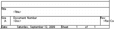
| 2. | Fill in the title block. | |||||||||||||||||||||||
| Scroll to the lower right corner of the window. You will find the title block for the drawing. The names delimited with angle brackets (<Title>, <Doc>, and <Rev Code>) are place holders. Double click on each of these and enter appropriate values. |
(Click to enlarge) | |||||||||||||||||||||||
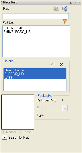
| 3. | Open Place Part Panel | |||||||||||||||||||||||
Click on the
Place Part
button
( ) in the toolbar.
This will bring up the
Place Part
panel.
This contains a list of the libraries that are available and the parts that they contain. ) in the toolbar.
This will bring up the
Place Part
panel.
This contains a list of the libraries that are available and the parts that they contain.
|
(Click to enlarge) | |||||||||||||||||||||||
| 4. | Select additional libraries. | |||||||||||||||||||||||
Click on the
Add Library
button
( )
in the Libraries box.
This will open a file select dialog on the directory containing the
builtin Cadence libraries.
Select "Connector.olb" and "Discrete.olb" and click
Open.
Notice that the
Parts List
has become much longer. )
in the Libraries box.
This will open a file select dialog on the directory containing the
builtin Cadence libraries.
Select "Connector.olb" and "Discrete.olb" and click
Open.
Notice that the
Parts List
has become much longer.
|
(Click to enlarge) | |||||||||||||||||||||||
| 5. | Place the first part. | |||||||||||||||||||||||
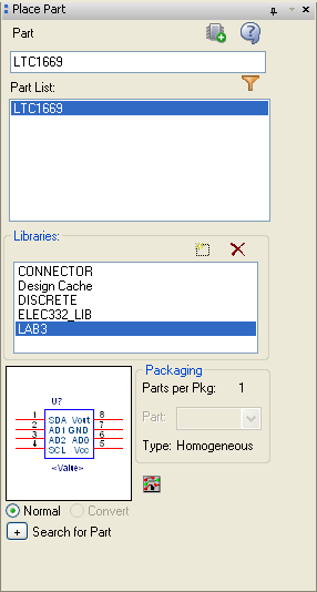
Select "LAB3" in the Libraries list,
then select "ST1669 in the Parts List.
The part you just created should appear iin the preview box at the bottom of the panel.
Click on the Place Part button
( )
at the top of the panel. )
at the top of the panel.
|
(Click to enlarge) | |||||||||||||||||||||||
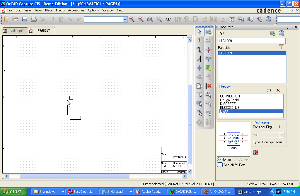
| Move the cursor into the drawing window. A skeleton of the part outline will appear, stuck to the cursor. |
(Click to enlarge) | |||||||||||||||||||||||
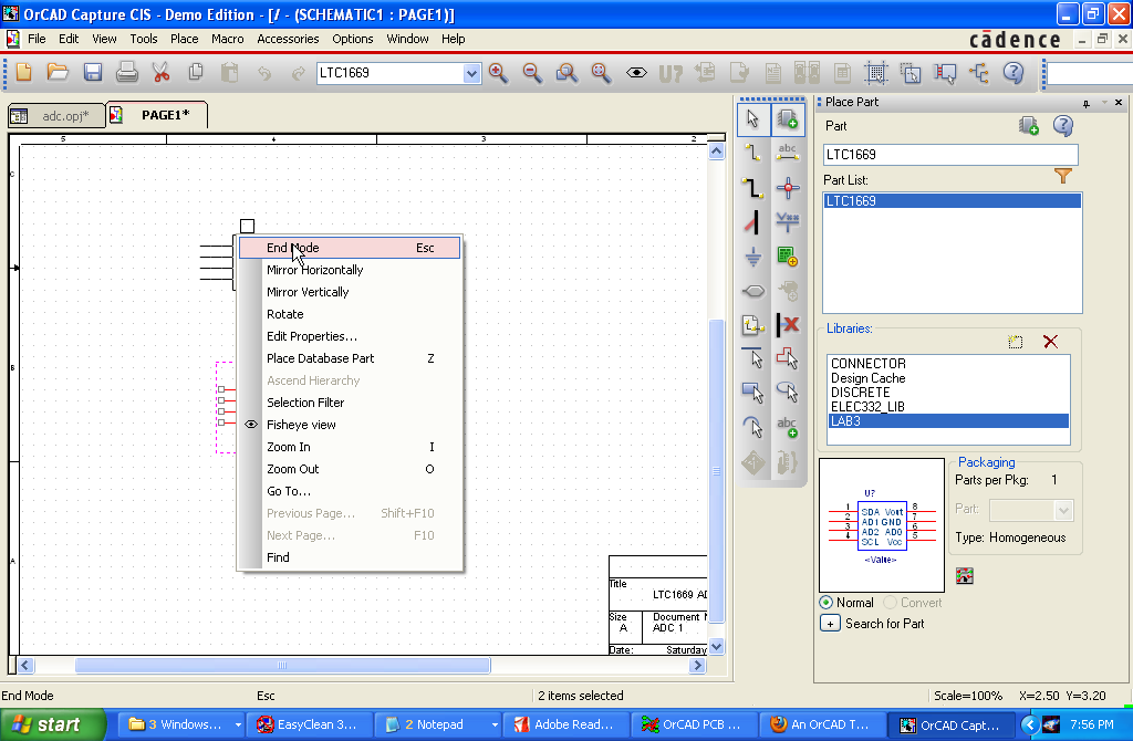
| Move the cursor to the center of the window and left click. A fully fledged copy of the part will be placed, and another skeleton will appear and follow the cursor. This is convenient for placing multiple copies of the same part, but we don't need to do that here. To stop this endless supply of parts, right click and select End Mode. You have placed your first part. |
(Click to enlarge) | |||||||||||||||||||||||
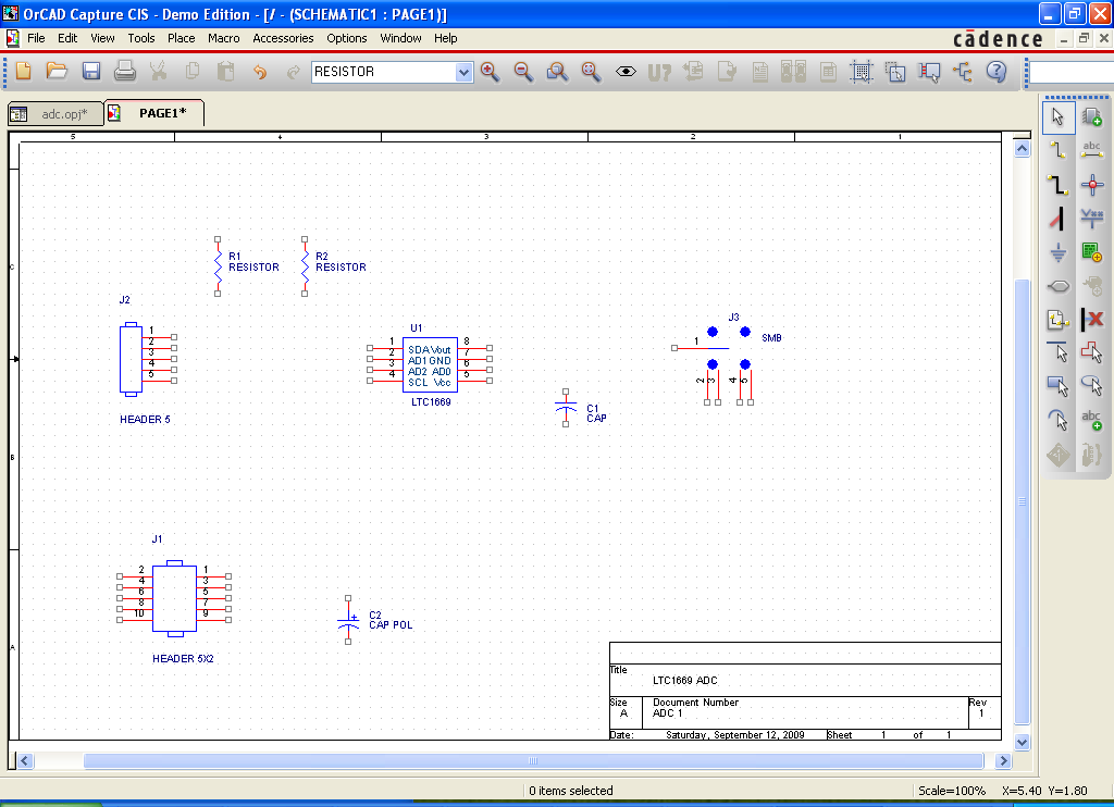
| 6. | Place the remaining parts. | |||||||||||||||||||||||
Repeat this process for the remaining components in the drawing,
selecting the correct library and part names.
If you get tired of exploring, here are some suitable choices:
| ||||||||||||||||||||||||
| 7. | Place ground and power symbols. | |||||||||||||||||||||||
The symbols for ground and power are so important that they have their own
buttons in the tool bar: "Place ground" ( )
and "Place power" ( )
and "Place power" ( ).
Clicking one of these brings up the "Place Ground" or "Place Power" dialog.
Select whichever symbol seems most appropriate and place it as you would a part. ).
Clicking one of these brings up the "Place Ground" or "Place Power" dialog.
Select whichever symbol seems most appropriate and place it as you would a part.
|
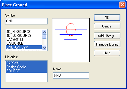
(Click to enlarge) | |||||||||||||||||||||||
| 8. | Clean up the window. | |||||||||||||||||||||||
| When you have finished placing all of the components, clik the "x" in the upper right corner of the Place Part panel. This will close the panel and create more room for the schematic. Components can be moved by selecting and dragging. Components can be rotated in increments of 90 degrees by typing "r" while selected. |
(Click to enlarge) | |||||||||||||||||||||||
| 9. | Make Connections | |||||||||||||||||||||||
| Note that each pin has a small square on the end of it. This shows that it is not connected and indicates the point to which a wire may be attached. |

| |||||||||||||||||||||||
Begin wiring by selecting the
Place wire
button ( ) from the toolbar.
When you reenter the schematic area, your cursor will become a crosshair.
When placed over a connection point, a rectangle will appear containing
the node or pin name.
This has two functions, the obvious one being that it identifies the node,
the useful one being that it indicates that left clicking at this point will
create a connection. ) from the toolbar.
When you reenter the schematic area, your cursor will become a crosshair.
When placed over a connection point, a rectangle will appear containing
the node or pin name.
This has two functions, the obvious one being that it identifies the node,
the useful one being that it indicates that left clicking at this point will
create a connection.
|
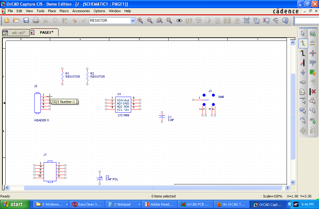
(Click to enlarge) | |||||||||||||||||||||||
| Once the first end of the wire is connected, the other end will follow the cursor, making right angle bends as necessary. When the free end is placed over a connection point (indicated by the appearance of the name box) it may be connected by left clicking. Left clicking when not over a connection point will put a corner in the wire's path at that point, but the wire will continue to be active until clicked over a connection point, or until right clicking and selecting End Wire. |
(Click to enlarge) | |||||||||||||||||||||||
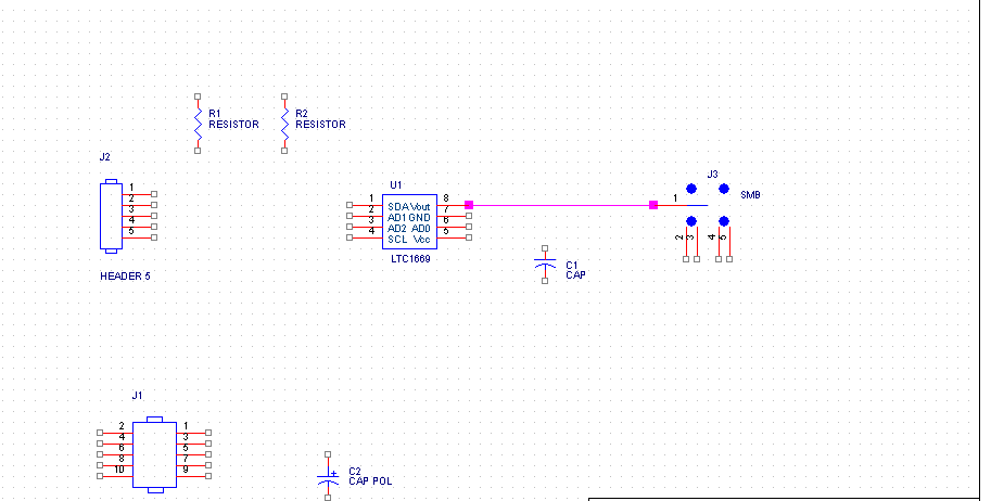
To avoid cluttering up the drawing with lots of long lines, it is often better
to form a connection by giving all of the pins on the same node the same signal
name.
To do this, connect a short piece of wire to the pin with the second end unconnected.
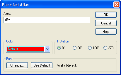
Select the "Place net alias" button ( ) from the tool bar.
The "Place Net Alias" dialog will appear.
Enter the name of the net and click
OK. ) from the tool bar.
The "Place Net Alias" dialog will appear.
Enter the name of the net and click
OK.
|
(Click to enlarge) | |||||||||||||||||||||||
| A small box will attach itself to the tip of the cursor. Move this box directly above the wire you wish to label and left click. A label will be placed at that point, but the box will remain stuck to the cursor. This is handy if you want to label several wires with the same signal name. If not, right click and select "End Mode." |
| |||||||||||||||||||||||
| Using these two techniques, continue until all connections have been made. | ||||||||||||||||||||||||
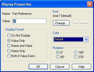
| 1. | Set part number. | ||||||||||||||||||
|---|---|---|---|---|---|---|---|---|---|---|---|---|---|---|---|---|---|---|---|
| As you place each component, a part number is automatically generated for it. If you're happy with this number, you can leave it alone. If it needs to be changed, double click on it to bring up the "Display Properites" dialog. Change the name, and click OK. |
(Click to enlarge) | ||||||||||||||||||
| 2. | Set PCB footprint. | ||||||||||||||||||
In order to mount a component onto the PCB, the pattern on the board
(called the
footprint)
must match the physical dimensions of the component.
Getting this wrong is one of the most frequent causes of grief in PCB layout.
This is where your stack of component data sheets comes in.
You should verify that the dimensions of each component match those of its footprint.
This is tricky at this poiint, as we have not seen the footprints yet.
To avoid having to jump around in our tutorial, we will use the following list:
| |||||||||||||||||||
| The way we set a footprint for a component is simple, but tedious. Double click over a component. This will open the property editor for the component. In the Filter by: field, select "Orcad Capture." |
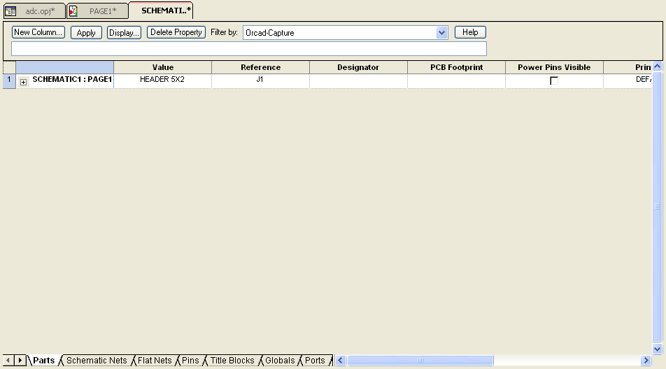
(Click to enlarge) | ||||||||||||||||||
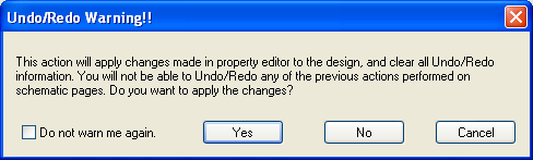
| Click in the "PCB Footprint" cell and type the name of the footprint. Right click in the tab labeled "SCHEMATI.." and select "Close." You will get an intimidating warning asking if you want to apply the changes. Answer "Yes" and it will go away. Repeat this for every component in the drawing. |
(Click to enlarge) | ||||||||||||||||||
| 3. | Save the drawing | ||||||||||||||||||
| Select "Save" from the "File" menu. |
| 1. | Bring up the project panel. | |||
|---|---|---|---|---|
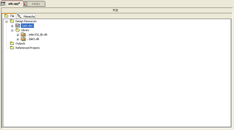
| Click on the leftmost tab, labeled "adc.opj" This will bring up the project panel for the design. |
(Click to enlarge) | |||
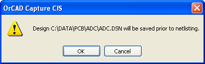
Select the "./adc.dsn" line, then click the
Create netlist
button ( ).
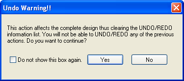
This will bring up another nasty warning message.
Just say "Yes." ).
This will bring up another nasty warning message.
Just say "Yes."
|
(Click to enlarge) | |||
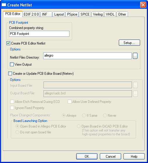
| Finally we get the "Create Netlist" dialog. The default values are what we want, so just click OK. |
(Click to enlarge) | |||
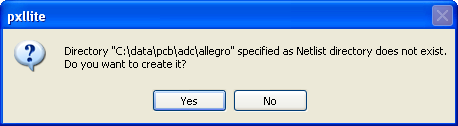
| Once again we get a warning which we have no choice but accept. |
(Click to enlarge) | |||
| And another ... |
(Click to enlarge) | |||
| Finally something happens |
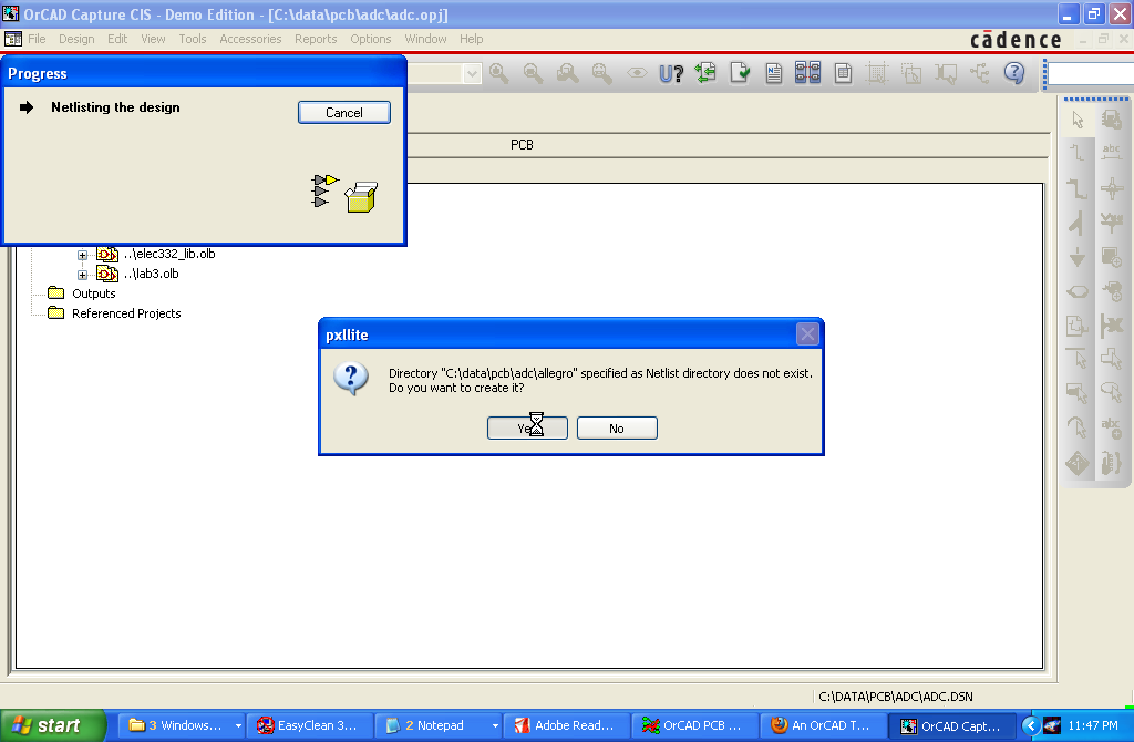
(Click to enlarge) | |||
| After all the warnings about things that are supposed to happen, there's no indication of a successful conclusion. If things go badly wrong, you will get an error message. For details, you can reenable the session log by clicking its box in the Window menu. Alternately, an explanation of what went wrong will be in the file <home>/pcb/adc/allegro/netlist.log | ||||
| At this point (assuming no mistakes in our circuit) schematic capture is done and we're ready to start layout. This is covered in the next section of the tutorial. |