Project Description
50 Word Description
Functional Description
Scoring Algorithm
Pin Count
Pin Map
Interactive Floor Plan
Old Block Diagrams
Timing Diagrams
FSM Timing Diagram
Input Timing Diagram
Logic Timing Diagram
Output Timing Diagram
FSM Design and MEG
FSM State Table
FSM Inputs and Outputs
FSM Magic Layout
FSM IRSIM
Major Blocks &
Subcells
Logic Diagram Links
Cell Hierarchy
Magic and IRSIM
Performance Analysis
IRSIM
Spice
Summary
About Us
Mid-Semester Status Report
|
|
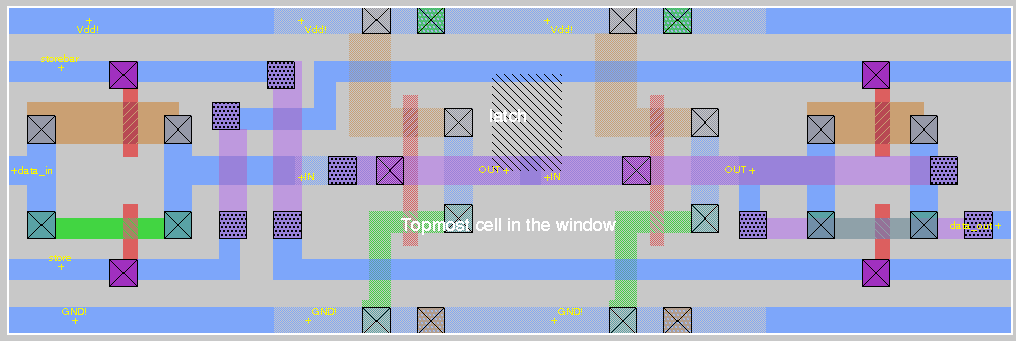
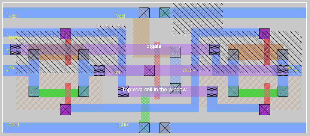
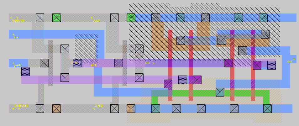
Major Blocks and Leaf Cells of the Design
|
Note: links are to logic diagrams
- Main PLA
finite state machine to control entire chip
- 8-bit Latch
latch key and guess
- 4-bit Barrel Shifter with Resetable Latch
manipulate guess and valid bits for key and guess
- 2-Bit Comparator (= or not =)
XOR, NAND2, NOR3
- Feedback Logic
control valid bits
INV, NAND2
- Summing Logic
PLA tool implements truth table
- 3-Bit Adder
used for running sum of whites, incrememter
- Low-Score Comparator
(less than or not less than)
- 1-Bit, 3-Bit, 4-Bit, and 8-Bit Latches with Resets, T-Gate
used for data storage, clocking control, temporary latching
|
Low-Level Subcells of the Design
|
|