To add components, click on Add in the menu banner of the schematic
entry window and choose Instance ( Add -> Instance )
Two new windows should appear.
One is the Add component window, where you can type in the
Library Name, Cell Name and the View Name of the
component to be added to the schematic (if you know it).
The other is the Component Browser window, where you can look
through your libraries for symbols to add to the schematic.
First we will select the MOS transistors from the Component Browser window.
Select the component library "analogLib" by clicking
and holding the left mouse button on the library field.
There are many entries in this library. To pick an n-type MOSFET, click on
click once on "nmos" (a model for a three terminal n-type MOSFET).
Move the mouse cursor on the schematic window to see a bright NMOS transistor
symbol moving with the mouse pointer. Decide where to put this transistor and
click on a location in the schematic window to place it.
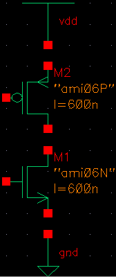
Do the same for the PMOS transistor. Pick "pmos" in the Component Browser
and place it on the schematic. Notice that the arror on the pmos transistor
points toward the gate.
Next place one instance of power (vdd) and one instance of ground
(gnd) on the schematic.
Now that you have placed the necessary components, type ESC to exit the
add component tool.
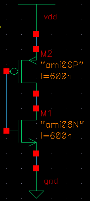
Now we will wire the components together. Type w or select Add
-> Wire (narrow) from the pull-down menus to bring up the wiring tool.
Connect vdd to the source terminal of the pmos transistor
by left clicking first on the red pin at the base of the vdd symbol and then
on the red pin at the top of the pmos symbol.
Now connect the drain of the pmos transistor to the drain of the nmos
transistor and connect the source node of the nmos transistor to ground.
Note: If you overlap the pins, the schematic editor will automatically connect them with nets.
Connect the two gates together and type ESC to exit the wire tool.
Now we will edit the properties of the transistors. Select Edit ->
Properties -> Objects q to bring up the form (or select the transistor
and type q, the bind key shortcut).
The following form should pop up. Note: the library name below
is incorrect, your library should be called analogLib
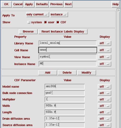
You may change the values for Width or Length depending on your design
specifications. Usually, you will change only the Width value,
which stands for the channel width, W (900n M is the minimum value for our
technology). The channel Length, L, defaults to 600 nanometers. The model name
specifies the hspice model used in hspice simulation.
Set the nmos transistor width to 900n M and the pmos transistor width to 600n M
for the present.
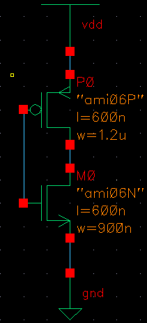
Now, to place the pins, click on Add -> Pin from the menus or type
p for the keyboard shortcut.
In the Add Pin window that appears, use a for the name of
the pin, make sure it is of direction input, and click on the schematic to place it. Now type y in the name field and create another pin of
direction output. Type ESC to escape the pin command and use the wiring command (w) to wire pin a to the gates of the transistors
and pin y to the drains of the transistors.
The pins can actually have any name you want to give them, but it is important
that the pin names agree in all views of the cell. I use the names a
and y because those pin names are used in the layout tutorial for the
inverter.
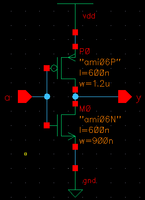
You have now finished the inverter functional schematic. Select Design -> Check and Save F8 from the menus (or type F8) and look in the CIW window for messages concerning errors. If you have errors correct them, otherwise you may exit the design by selecting Window -> Close.