blue v(5)=bout
The crystal command file is separated into four sections:
| input node | toggle | output node | result | delay (ns) |
|---|---|---|---|---|
| to aout | ||||
| ASEL | low | aout | low | 1.83 |
| ASEL | high | aout | high | 2.98 |
| ain | low | aout | low | 1.83 |
| ain | high | aout | high | 3.37 |
| Addition: bin to bout | ||||
| bin | low | bout | low | 5.91 |
| bin | high | bout | high | 11.16 |
| Subtraction: bin to bout | ||||
| bin | low | bout | high | 15.77 |
| bin | high | bout | low | 10.66 |
| Multiplication: to bout | ||||
| -MRESET | low | bout | low | 6.23 |
| -MRESET | high | bout | high | 8.55 |
| fsum | low | bout | low | 6.23 |
| fsum | high | bout | high | 8.94 |
| Feedback: sumin to fsum | ||||
| sumin | low | fsum | low | 5.57 |
| sumin | high | fsum | high | 8.35 |
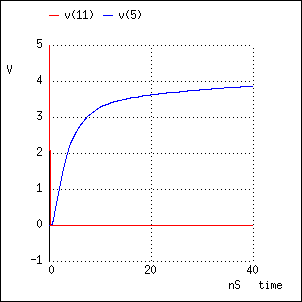
crystal determined that bin switching low during a subtraction operation created the longest path: bout switched high after 15.77 ns. crystal was used to generate a SPICE input file, which in turn was used to generate the following graph:
red v(11)=bin
blue v(5)=bout

(The above graph is also available in .ps format.) bout appears to be asymptotically approaching 4 V. If this is true, it achieves 90% of its final value after about 15 ns. We are not sure why bout does not approach a full 5 V.
The crystal command file for the carry lookahead adder toggled each possible input bit to the adder in turn, looking for the longest path to any of the sum output bits, or the two high order carry-out bits (which are used in the calculation of overflow).
| input node | toggle | output node | result | delay (ns) |
|---|---|---|---|---|
| cin | high | c3 | high | 16.41 |
| cin | low | s3 | high | 18.35 |
| a0 | high | s3 | high | 29.61 |
| a0 | low | s3 | low | 29.35 |
| a1 | high | s3 | high | 30.25 |
| a1 | low | s3 | low | 29.92 |
| a2 | high | s3 | high | 29.05 |
| a2 | low | s3 | low | 30.09 |
| a3 | high | c3 | high | 23.17 |
| a3 | low | c3 | high | 24.31 |
| b0 | high | s3 | high | 29.22 |
| b0 | low | s3 | low | 29.35 |
| b1 | high | s3 | high | 29.85 |
| b1 | low | s3 | low | 29.92 |
| b2 | high | s3 | high | 28.66 |
| b2 | low | s3 | low | 30.09 |
| b3 | high | c3 | high | 23.17 |
| b3 | low | c3 | high | 24.31 |
crystal determined that if a1 is driven high, in the worst case, s3 will be driven low 30.25 ns later. The crystal-generated SPICE input file generated the following graph:
red v(41)=a1
blue v(5)=s3
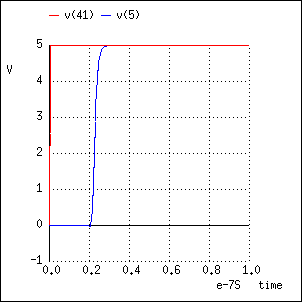
(The above graph is also available in .ps format.) s3 reaches 90% of its final value at about 25 ns.
A crystal command file observed the paths from the input to both the latched and the gated outputs. For the latched output, ph2 is held high. For the gated output, ADDOUT is held high.
| input node | toggle | output node | result | delay (ns) |
|---|---|---|---|---|
| Latched output: sumin to ssum | ||||
| sumin | low | ssum | low | 5.11 |
| sumin | high | ssum | high | 7.89 |
| Gated output: sumin to sumout | ||||
| sumin | low | sumout | low | 5.11 |
| sumin | high | sumout | high | 7.89 |
crystal determined that the longest paths through the latch and the gate are both 7.89 ns, and both occur when sumin is driven high. The crystal-generated SPICE input file generated the following graph:
red v(11)=sumin
blue v(5)=ssum
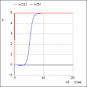
(The above graph is also available in .ps format.) ssum achieves 90% of its final value after about 7 ns.
A crystal command file was used to investigate the longest path through the entire block. For the purposes of determining the maximum clock speed, we must find the longest path from the outputs of the input latches to the outputs of output latches. In all cases, the input latches for the feedback values and MRESET (the a and b latches are external to the adder) are turned off (ph1 is held low) and crystal drives the rest of the circuit from the outputs of these latches. CO and OVERFLOW are latched inside the adder, but the outputs are not. A new magic file containing the adder and the output register was used for the simulation. crystal found the longest path to any of the latched output bits (out[15:8], CO, or OVERFLOW) when each input bit was toggled.
For addition and subtraction, OP4 was asserted. For multiplication, OP4 and OP0 were deasserted. In all cases, ADDOUT and LATCHOUT were asserted to enable the output gates and latches.
| input node | toggle | output node | result | delay (ns) |
|---|---|---|---|---|
| Addition or subtraction | ||||
| a0 | low | out15 | high | 95.72 |
| a0 | high | out15 | high | 101.37 |
| a1 | low | out15 | high | 96.56 |
| a1 | high | out15 | high | 102.01 |
| a2 | low | out15 | high | 98.04 |
| a2 | high | out15 | high | 102.27 |
| a3 | low | out15 | high | 97.00 |
| a3 | high | out15 | high | 100.85 |
| a4 | low | out15 | high | 65.88 |
| a4 | high | out15 | high | 71.53 |
| a5 | low | out15 | high | 66.72 |
| a5 | high | out15 | high | 72.16 |
| a6 | low | out15 | high | 66.94 |
| a6 | high | out15 | high | 71.17 |
| a7 | low | OVERFLOW | high | 57.97 |
| a7 | high | OVERFLOW | high | 61.83 |
| b0 | low | out15 | high | 120.74 |
| b0 | high | out15 | high | 114.89 |
| b1 | low | out15 | high | 121.38 |
| b1 | high | out15 | high | 115.53 |
| b2 | low | out15 | high | 121.64 |
| b2 | high | out15 | high | 115.79 |
| b3 | low | out15 | high | 120.22 |
| b3 | high | out15 | high | 114.37 |
| b4 | low | out15 | high | 90.90 |
| b4 | high | out15 | high | 85.05 |
| b5 | low | out15 | high | 91.53 |
| b5 | high | out15 | high | 85.68 |
| b6 | low | out15 | high | 90.54 |
| b6 | high | out15 | high | 84.69 |
| b7 | low | OVERFLOW | high | 81.19 |
| b7 | high | OVERFLOW | high | 75.34 |
| Multiplication | ||||
| f0 | low | out15 | high | 97.84 |
| f0 | high | out15 | high | 80.20 |
| f1 | low | out15 | high | 100.49 |
| f1 | high | out15 | high | 109.03 |
| f2 | low | out15 | high | 103.41 |
| f2 | high | out15 | high | 111.08 |
| f3 | low | out15 | high | 102.37 |
| f3 | high | out15 | high | 109.67 |
| f4 | low | out15 | high | 71.25 |
| f4 | high | out15 | high | 80.34 |
| f5 | low | out15 | high | 72.09 |
| f5 | high | out15 | high | 80.98 |
| f6 | low | out15 | high | 72.31 |
| f6 | high | out15 | high | 79.98 |
| f7 | low | OVERFLOW | high | 63.35 |
| f7 | high | OVERFLOW | high | 70.64 |
| b0 | low | out15 | high | 105.71 |
| b0 | high | out15 | high | 108.45 |
| -MRESET | low | out15 | high | 103.41 |
| -MRESET | high | out15 | high | 110.69 |
crystal determined that the longest path occurs when b2 is driven low: out15 is driven high 121.64 ns later. The crystal-generated SPICE input file generated the following graph:
red v(71)=b2
blue v(5)=out15
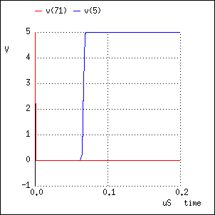
(The above graph is also available in .ps format.) out15 achieves 90% of its final value after about 70 ns.
crystal found the longest path through the entire adder (including output latches) to be 121.64 ns. This represents the minimum time from ph1 fall to ph2 fall. If the time from ph2 fall to ph1 is the same, the total period is 243.28 ns for each clock. The maximum clock speed is the inverse of this value: 4.11 MHz. If the time from ph2 fall to ph1 is reduced to the minimum value of 8.35 ns (as found in the analysis of the input bit selector), the total period is 129.99 ns, and the maximum clock speed is 7.69 MHZ.
SPICE simulated the longest path through the entire adder with a rise time of about 70 ns. If the two phases are of equal length, the total period is 140 ns and the maximum clock speed is 7.14 MHz. If the second phase is shortened to about 10 ns to allow the feedback value to latch, the total clock period is 80 ns and the maximum clock speed is 12.5 MHz.
If the adder is the limiting factor of the chip, it should easily be capable of running at 4 MHz, and possible as high as 7 MHz, with equal phase clocks. If we shorten the second phase, it should be able to achieve speeds of 7 to 12 MHz.
I did not realize that crystal could be provided with a single long list of delay statements and remember the longest critical path. Therefore, my crystal command files consist of many sets of setup commands, each followed by a single delay command. This also resulted in a large quantity of data to be filtered, as is evidenced by the tables above. The whole process could have been simplified immensely, and the quantity of data reduced.