Previous Tutorial
Main Menu
Next Tutorial
Design Extraction
To verify the functionality and timing of this inverter, you need to extract the spice
netlist from the layout then simulate it. Unfortunatly, the netlisting is not working at the
moment, but we can still generate the extracted view from which a netlist can be generated
(once we fix the installation).
The extracted view also allows you to run LVS (Layout vs Schematic). This tool (which is also
not working at the moment, probably for the same reason the netlisting is broken) allows you
to compare a schematic and an extracted physical layout to verify that they are equivalent (
i.e. signals are connected the same way).
To generate the extracted view,
-
Start Cadence using "icfb".
-
Open layout view of the inv you created in the layout tutorial for editing.
-
In Virtuoso Editing window, select Verify ->
Extract...
An Extractor form appears.
-
Make sure that Extract Method is "flat", Rule File
is "divaEXT.rul" and Rule Library is NCSU_Techlib_ami06".
-
Click Set Switches and select "Extract_parasitic_caps", then
click "OK" on Set Switches Window.
-
Click "OK" on Extractor Window.
Cadence extractor will extract the layout and save it as extracted
view. You can see the extracted view appear in Library Manager
window under inv. You may close the layout view now.
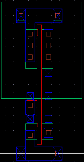
Let's take a close look at the extracted view first.
-
Open extracted view of inv for editing. The extracted view looks
similar to the layout view. You should notice that there are no
nselect and pselect in extracted view. Try right-clicking on
part of the layout. Everything electrically conected to the point you choose
should become highlighted.
-
The extracted view contains devices extracted from layout view.
From Virtuoso menu, select Window -> Zoom In,
then click on (1.50, 4.20) and then (2.70, 3.00). You will see a "nmos4"
which means 4 terminal nmos transistor which was extracted from your layout
view.
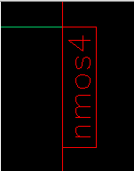
Comment: Always search the upper left corner of the transistor gates
for the extracted transistors.
-
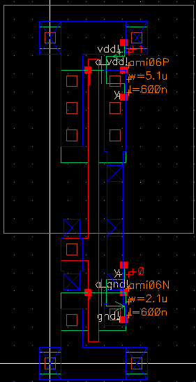
From Virtuoso menu, select Design ->
Option
-> Display... e This brings out an Editor Option window.
Change Display Level from 0 to 20 then click "OK". It expands the
display level and gives you an nmos symbol with node names (y,
a
and gnd!), instance name (0) and device parameters (w,
l).
Comment: Bind key to expand Display Level to 20 is "shift-f". Bind
key to change Display Level back to 0 is "Control-f".
-
From Virtuoso menu, select Window -> Fit All f
You will see a pmos transistor and a paracitic capacitor. Please take some
time identify the node names (in, vdd!,
gnd!, and
out),
instance names(1 which is the pmos and 0 is the nmos) and
device parameters (w and l)
Refer to 'Diva: Interactive Design Rule Checking' for more information
about DRC and extraction.
Previous Tutorial
Main Menu
Next Tutorial