Previous Tutorial
Main Menu
Next Tutorial
Generating Abstract View for Silicon Ensemble
Unfortunatly the abstract view created in Virtuoso does not include some
important information required by Silicon Ensemble, so this intermediate step
helps in moving the design between programs.
Export GDS
Abstract generator comes as a part of the Silicon Ensemble package. As such,
it cannot directly read ICFB library databases. We need to export the standard
cell library to Stream (GDS) format, then re-import the GDS file in Abstract
Generator.
To export to GDS format from ICFB:
- Go to the CIW.
- Click on File -> Export -> Stream...
- In the Virtuoso Stream Out form, enter the following information:
- Run Directory: .
- Library Name: tutorial
- Top Cell Name: (leave blank)
- View Name: layout
- Output File: library_name.gds
- Then, click on the User-Defined Data button. A new form, the Stream-Out
User-Defined Data form will appear.
In the Stream Out User-Defined Data form, enter stream.map for the
Layer Map Table. Then, click on OK.
The text file stream.map tells ICFB which
layers correspond to which GDS numbers. Copy this file into your cadence
directory. When we re-import the GDS file back into Abstract Generator, the tech file
we are going to use has the same layer mappings.
Now, back in the Virtuoso Stream Out form, click on the Options
button.
A new form, the Stream Out Options form, will appear.
In the Stream Out Options form, select No Merge for the Convert
PCells to Geometry field. This flattens out any parametric cells in the
cell library (For the I/O Pad Cells). Then, click on OK.
Click on OK in the Virtuoso Stream Out form. A GDS file containing the standard
cell library will be generated. (There will probably be some warnings and possibly an error, but you can usually ignore them.)
Initialize Abstract Generator
Before we use Abstract Generator, we need to set it up so that it uses our
technology file (i.e. ami06 technology).
First create a directory for
Silicon Ensemble with a subdirectory called tech
Copy this
file into your tech directory and name it tech.dpux.
Start the Abstract Generator by typing abstract -tech ./tech
in your Silicon Ensemble directory. First we will add your library to
the technology file (tech.dpux) inside of Silicon Ensemble's Abstract Generator.
Begin by clicking on File -> Technology... to bring up the
Technology File Editor. Under Categories (on the left), click on Library Path.
Click on Add and replace newLib1 with the name of your library (e.g. mylib) and
newPath with the path to your cadence library (e.g. /home/usr_name/cadence/mylib)
I would recommend having one library for each of your local Viruoso design libraries
(but not the system-wide libraries) and have the library path point
directly to the Cadence version of the library. The Silicon Ensemble abstract
version of the cells will show up in ALL CAPS in Virtuoso, but the views will
not be readable by Virtuoso. If your cells are named using ALL CAPS in Virtuoso,
you will need to make a seperate library directory for you abstract generator cells.
In the Technology File Editor window, click on File
-> Save and close the Technology File Editor window.
Using Abstract Generator
Next we will be importing the GDS file exported earlier from Virtuoso.
In the main window click on File -> Library. Since you only have one
Library at this point it should come up automatically.
Click on File -> Import -> Layout and
browse until you find the GDS file you exported earlier from Virtuoso. Then
click OK.
After a few moments the cells from your library will
appear in the window in bin Core.
At this point, if there are any cells that do not have a green check next to
them in the layout view, select them (Shift allows you to select groups,
Control allows you to select or deselect one at a time...same as windows).
When they are all selected, click on Cells -> Move The Move Select
Cells form will appear, click on the ignore bin and OK to
move these cells to the Ignore bin.
Note: If there are cells without any valid views in the Core bin, you may
not be able to export the library later.
To see what your cells look like in the Abstract Generator, make sure that you
are in the Core bin, select the cell you would like to view, and click on
Cells -> Edit -> Layout...
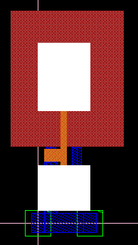
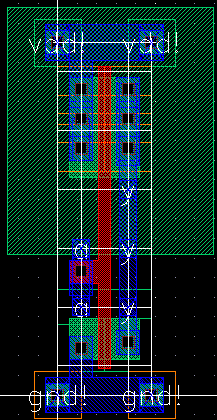
The inverter cell (created in the layout tutorial) should look something
like this:
Because we are only interested in the metal and via layers, lets make them
visible
- In the layout editing window, click on View -> Layers This will
invoke and Layer Editor form
- First, click on the None button beside the Visible field.
This turns all layers invisible
- Next, in the Layer-Purpose column, find the metal1 drawing
entry. Click on it once, then check the Visible checkbox.
- Now do the same for the other purposes of metal1 (metal1 pin,
metal1 net, and metal1 boundary).
- Do the same for all layer-purposes of metal2 and Text as
well (and metal3 if you have any in your design).
- Click on the Redraw button, then the Close button. The
Layout Editing window will now only show the metal and text layers.
Note: All other editing windows you open after this will now only show metal
and text layers (unless you edit the layers again or exit the program)
There are three main steps in generating abstracts - generating the Pins view, the Extract view, and finally the Abstract view.
- The Pins step maps text labels to metal layers, designating certain metal blocks as pins (all pin information is lost during GDS export, so we need to re-instate that information).
- The Extract The Extract step merges metal blocks under the same net into one single net (we will not be using this function since we want our pins to be specifically 3x3 lambda sized pins). It also changes any metal.pin layer into metal.net.
- The Abstract step copies the pin (net) information from the Extract step, and generated blockages for the metal and via layers (or any other layer that you specify). These blockages will tell the place-and-route tool (namely Silicon Ensemble) which parts of the standard cell to avoid routing over with certain layers.
The resulting Abstract view contains only net and blockage information, which will be exported into an LEF file and imported into Silicon Ensemble.
Pins Step
If all of your cells are alike, you can process them all at once, but for now
we will use the INV from the layout tutorial as an example.
Select INV and click on Flow -> Pins.
The Pins form will appear.
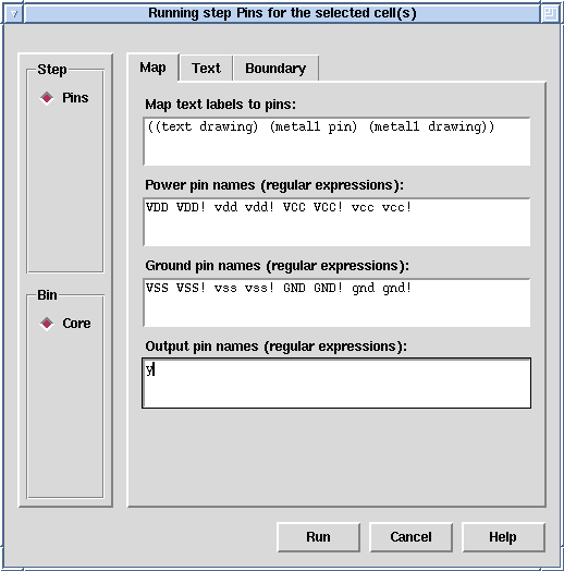
Under Map Text label to Pins we entered ((text drawing) (metal1 pin) (metal1 drawing))
This tells Abgen to map any text in text.drawing to metal1.pin shapes if there
are any metal1.pin shapes overlapping the text.
If there are not any metal1.pin shapes overlapping the text, then map the text to any
overlapping metal1.drawing shapes.
This works if all of your text labels are either located over metal1.pin shapes
(for your regular pins), or over metal1.drawing shapes (for your vdd/gnd pins).
If you have metal2 pins, you might try
((text drawing) (metal1 pin) (metal2 pin) (metal1 drawing) )
Under Power pin names are all of the possible nets that specify power
(we only use the vdd! net).
Under Ground pin names are all of the possible nets that specify ground
(we only use the gnd! net).
Under Output pin names is where you list the names of any output pins
in the cells you are abstracting (e.g. y is the output of the inverter
created in the layout tutorial) In the exported LEF file, these pins will
have "output" as their direction.
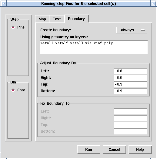
The Pins step also generates Place-and-Route Boundaries (PR Boundaries) for
each cell.
-
Click on the Boundary tab. The Pins form will change to one shown above.
-
Choose always for the Create Boundary field.
-
Fill in the values for Adjust Boundary By according to that shown above.
We are doing this because our inverter cell extends beyond the actual PR
Boundary (Refer back to the inverter layout)
This may not be the case for all of your cells, so adjust accordingly when
necessary.
- Now click on Run. When Abgen is done, you will see an excamation
mark beside INV in the Pins column. This means that there was a
warning (not an error) in the generation of that view.
- To view the warning click on Cells -> Report (with INV selected)
The warning should state that the PR Boundary for INV does not enclose
all cell view geometry. This is okay, since we know we have some geometry that
extends beyond the cell's PR Boundary.
- Click OK to close the report window.
- If you wish to view the pin view, click on Cells -> Edit -> Pins
Extract Step
- After selecting INV, click on Flow -> Extract
- De-select the Extract Signal Nets box
- Click on the Power tab and de-select Extract Power Nets
- Click on Run to extract the cell
- If you wish to see the extract view, click on Cells -> Edit -> Extract
Abstract Step
- After selecting INV, click on Flow -> Abstract
- Under the Blockage tab, make sure that metal1 metal2 metal3
via via2 is entered for the Create detailed blockages on layers
field.
- Under the Site tab, enter core for the site name.
There are 4 pre-defined sites defined at the end of the NCSU lib file
ncsu_ami06_abgen.lef used to create our abstract tech file.
-
Site core is used for cells inside the pad frame that are 18um high
and some multiple of 2.4um wide.
- Site dbl_core is for cells 36um high and a multiple of 2.4um wide.
- Sites IO and corner describe components of the pad
frame.
Your cells must belong to one of the first two sites for successful
autorouting, because during the autorouting process cells are placed in
rows based on their site declaration. It is also possible to define other
sites by adding to the ncsu_ami06_abgen.lef file, but then you need to create
a new technology file for the Abstract Generator that includes these sites.
- Click on Run to generate the abstract view of INV
- The Abstract column should have an exclamation point, so click on
Cells -> Report to see the cause of the warning.
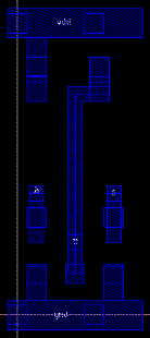
- The warning under the abstract step should state that vdd! and
gnd! have no pins on the Matal1-Metal2 routing grid. Referring back to the
layout shows that this is true, because we
have a horizontal grid offset.
This warning can be ignored because we are
not going to route vdd! and gnd!, since they are abutment pins.
Note: Warnings are not the same as errors. Whenever you encounter a warning,
look at the report to make sure that it was what you intended to do. If it is not, fix the problem before proceeding.
Always take a cell (or group of cells) all the way through the process before
going back and processing cells with different options in the forms (e.g. Pins
form). When abgen detects changes in form options, it will try to re-run the
preceeding steps again using the most recent options.
Cell Orientation
When all of the cells in the core bin that you wish to process have abstract views, it is time to set the correct properties.
Select the inverter cell and click on Cells -> Cell Properties
Make sure the bin is Core, the site is core, and symmetry
property is X Y (this means they can be flipped across both the X and Y
axis). Then click OK.
LEF File
There is one last step before exporting the LEF. Select General Options
under the File menu and choose Silicon Ensemble for Target
place and route system, 100 for LEF units, and 5.3 forLEF version. Click OK.
In the main window click on File -> Export -> LEF to bring up the
Export LEF form.
Specify the location of where you wish to save the
file.
Select Core fro the Export LEF for Bin field and click on OK.
This LEF file will be imported into Silicon Ensemble in the next section of this tutorial.
Previous Tutorial
Main Menu
Next Tutorial