Interactive Floor Plan
Timing Diagrams
FSM Design and MEG
Major Blocks & Subcells
Performance Analysis
Summary
About Us
Based upon HSPICE simulations of the surmised longest path, the estimated
clock
frequency for the chip is 67MHz. (see calculations
below)
This surprisingly fast clock frequency is the result of the A
and B clocking scheme,
which alternates the use of qualified A and B
signals on frequent latches that
propigate data through the chip. The
longest delay between A and B clocking is found
when data passes
through the extensive combinational logic of the Logic PLA. This
critical path connects the output of the guess and key comparison
latches, which are
latched on clock A, to the output latches of the Logic PLA,
which are latched on clock B.
The rise time of the Logic PLA outputs, as seen below, is longer than the
fall time.
clock A -> clock B
Rise time: 15.5-8.03 = 7.47nS
T = longest path * 2 = 14.94nS
1/T = frequency = 66.93 MHz
|
|
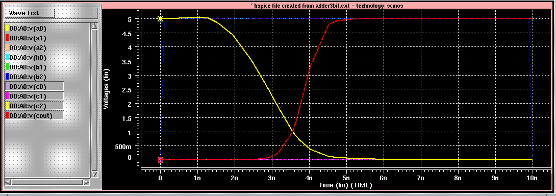
HSPICE simulation of the 3-bit Ripple-Carry Adder reveals a longest path of
6.2nS.
The following plot simulates the situation requiring a carry to
propigate throughout the
entire adder. Just like with the critical path analysis above, the
outputs of the adder
must be valid for latching on clock B. This gives the
following clock frequency, which
is faster than the above calculated
frequency and consistent with the previous
assumption that the above
path is the most critical path of the chip.
clock A -> clock B
Fall time: 6.3-.01 = 6.2nS
T = 6.2*2 = 12.4ns
1/T = frequency = 80.65MHs > 67mHz
|
|