
Contact Information
Rice University
6100 Main Street
Houston, Texas 77005, USA
Email: aydin.babakhani AT rice.edu
Tel: (713) 348-3821
Fax: (713) 348-5685
Current Research
Gone in a Picosecond: Techniques for the Generation and Detection of Picosecond Pulses and Their Applications, "
in IEEE Microwave Magazine, 2016.
This paper provides an overview of our recent work on silicon-based THz pulse technology and their applications.
A Nonlinear Q-Switching Impedance Technique for Picosecond Pulse Radiation in Silicon, "
in IEEE Transactions on Microwave Theory and Techniques, 2016.
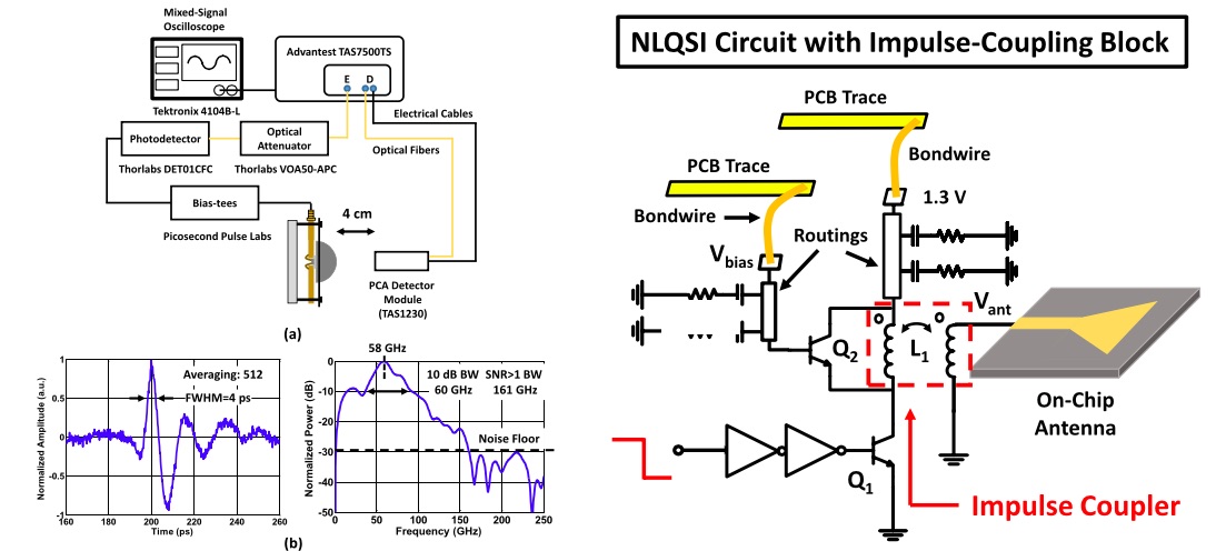
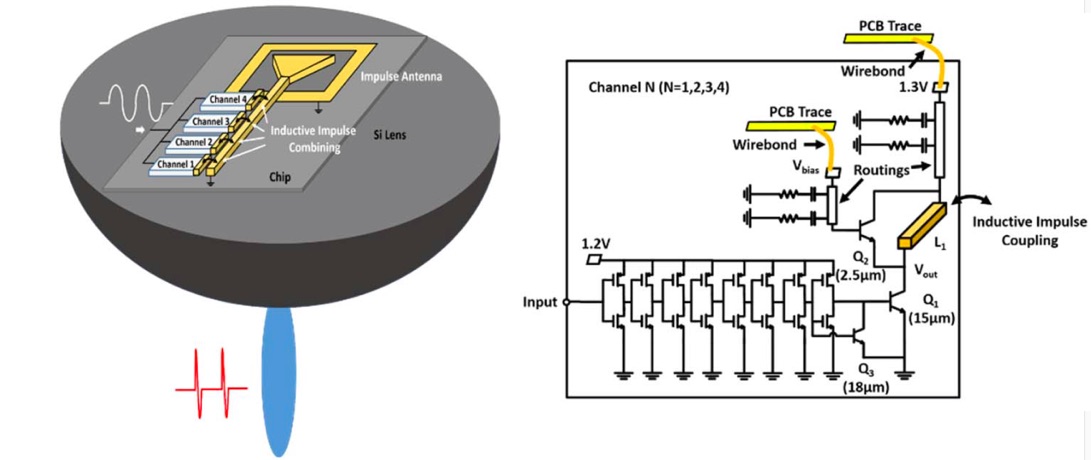
This paper presents a nonlinear Q-switching impedance (NLQSI) technique for picosecond pulse radiation in silicon. A prototype chip is designed with four NLQSI-based impulse generation channels, which can produce picosecond pulses with a reconfigurable amplitude. An on-chip impulse-coupling scheme combines the outputs from four channels and delivers the combined signal to an on-chip antenna. In addition, an asynchronous optical-sampling measurement system is used to characterize the radiated picosecond pulses in the time domain. The prototype chip can radiate 4ps pulses with an SNR > 1 bandwidth of 161 GHz. Furthermore, pulse amplitude modulation is experimentally demonstrated. The prototype chip is fabricated in a 130nm SiGe BiCMOS process technology with a die area of 1 mm2.
A Full-Duplex Single-Chip Transceiver with Self-Interference Cancellation in 0.13µm SiGe BiCMOS for Electron Paramagnetic Resonance Spectroscopy, "
in IEEE Journal of Solid State Circuits, 2016.
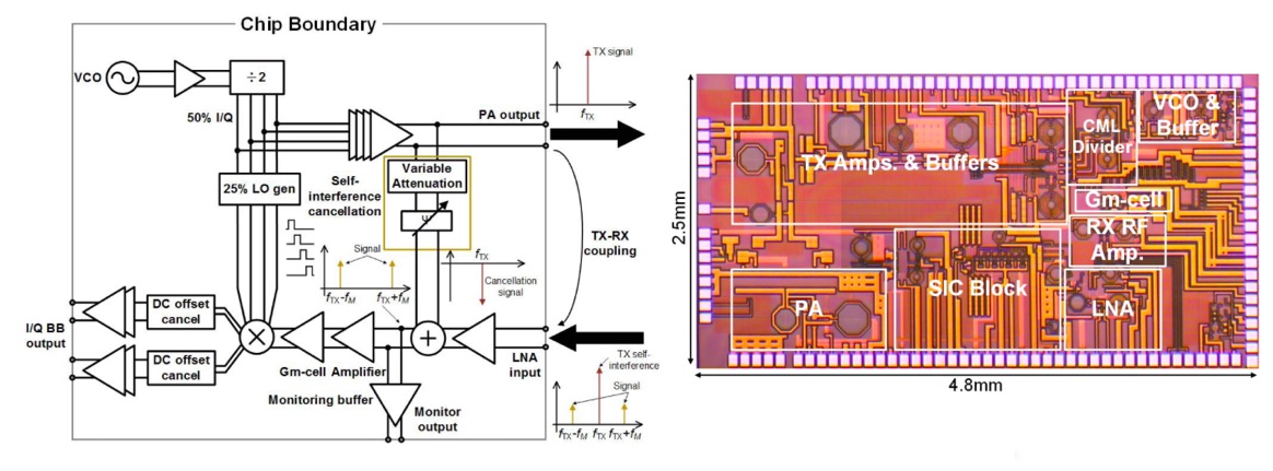
This paper presents a miniaturized EPR spectrometer based on a single-chip transceiver. Utilizing a novel on-chip self-interference cancellation circuit, the electromagnetic coupling from the transmitter (TX) to the receiver (RX) is minimized, allowing simultaneous achievement of large TX output power and low RX noise figure (NF). In the measurement, the RX achieves a NF of 3.1 dB/6.3 dB at 10 MHz/50 kHz baseband frequencies, when the TX and cancellation circuits are turned off. The measured flicker noise corner is 60 kHz, more than 10× lower than the prior work. Moreover, for the first time, the operation of the RX and cancellation circuit is demonstrated when a co-integrated TX is operating at the same time and frequency, while producing >20 dBm output power. When the TX and cancellation circuits are turned on, at -10 dBm interference power, the measured NF is 6.8 dB/11.1 dB at 10 MHz/50 kHz baseband frequencies. This is lower by 5.6 dB/9.6 dB at 10 MHz/50 kHz baseband frequencies, compared to the NF with the cancellation circuit off at the same interference power. The transceiver chip is implemented in IBM 0.13 µm BiCMOS process and consumes a power of 2 W. Utilizing this transceiver, an electron paramagnetic resonance (EPR) spectrometer is built and tested. It is observed, through measurement, that the interference cancellation circuit increases the signal-to-noise ratio (SNR) of the EPR signal by 7 dB at -10 dBm interference power. Compared to prior work, the reported EPR spectrometer improves the sensitivity of the system by 25 dB.
A Fully Integrated Electromagnetic Energy Harvesting Circuit with an on-Chip Antenna for Biomedical Implants in 180 nm SOI CMOS, "
in IEEE Sensors, Nov. 2016.
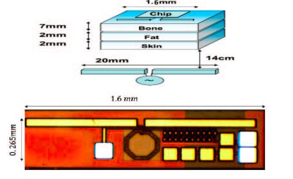
This paper presents an energy harvesting platform for biomedical implantable sensors based on a far-field electromagnetic radiation. The design is composed of an on-chip dipole antenna and a multi stage Dickson voltage rectifier with threshold compensation order of 4. The operating range is up to 15 cm, including 1 cm of biological tissue with high water content. The optimum frequency for power transmission into the implanted chip through multiple biological tissues is studied as well. The system is fabricated in a 180 nm SOI CMOS technology with a total area of 0.42 mm2. The chip can provide 1V DC for a 1MΩ resistive load when excited with an 11.2 GHz external transmitter. The maximum efficiency of the wireless link is measured as -51 dB. The voltage rectifier can provide 1V for the 1Mohm load with input power as low as 23 µW (-16.3 dBm).
Broadband THz Spectroscopic Imaging based on a Fully Integrated 4x2 Digital-to-Impulse Radiating Array with a Full-Spectrum of 0.03-1.03THz in Silicon, "
in IEEE Symposia on VLSI Technology and Circuits, Jun. 2016.
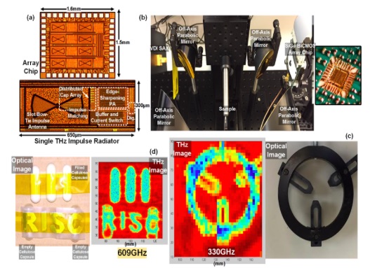
This paper presents a broadband THz frequency-comb spectroscopic imager based on a fully-integrated 4×2 picosecond Direct Digital-to-Impulse (D2I) radiating array. By employing a novel trigger-based beamforming architecture, the chip performs coherent spatial combining of broadband radiated pulses and achieves an SNR>1 BW of 1.03THz (at the receiver) with a pulse peak EIRP of 30dBm. Time-domain radiation is characterized using a fsec-laser-based THz sampler and a pulse width of 5.4ps is measured. Spectroscopic imaging of metal, plastic, and cellulose capsules (empty and filled) are demonstrated. This chip achieves signal generation with an available full-spectrum of 0.03-1.03THz. The 8-element single-chip array is fabricated in a 90nm SiGe BiCMOS process.
An Integrated Germanium-Based Optical Waveguide Coupled THz Photoconductive Antenna in Silicon, "
in the Conference on Lasers and Electro-Optics (CELO), Jun. 2016.
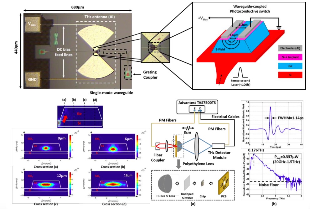
An integrated germanium-based optical waveguide coupled THz photoconductive antenna in a low-cost SOI process is presented with potentials to perform THz beam-steering. The radiated THz pulses achieve a FWHM of 1.14ps and bandwidth of 1.5THz.
Terahertz Trace Gas Spectroscopy Based on a Fully-Electronic Frequency-Comb Radiating Array in Silicon, "
in the Conference on Lasers and Electro-Optics (CELO), Jun. 2016.
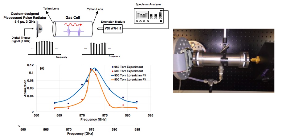
A silicon integrated circuit is reported for radiating picosecond pulses with tunable repetition rate, covering frequencies from 0.03 to 1.03 THz. This source is used in a gas spectroscopy setup to measure the absorption lines of ammonia and water in the terahertz region.
Broadband Beam-forming of Terahertz Pulses with a Single-Chip 4x2 Array in Silicon, "
in IEEE Antennas and Propagation International Symposium, Jun. 2016.(Best Paper Award-2nd Place)
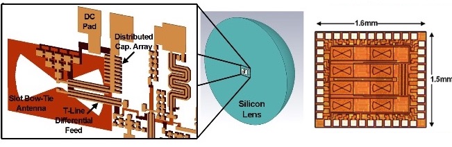
In this paper, a single-chip impulse antenna array is presented that performs spatial combining of picosecond impulses radiated from 8 elements. A new broadband beamforming architecture is introduced that controls the timing of impulses radiated from each antenna by delaying a trigger signal, with resolution steps of 300fsec. This method eliminates the distortive and narrowband effects of delay blocks in conventional phased arrays by separating the delay path from the information path. Frequency domain measurements are performed up to 1.03THz and array directivities of 22dBi at 0.33THz, 25dBi at 0.57THz, and 27dBi at 0.75THz are achieved. The 8-element array is fabricated in a 90nm Silicon Germanium BiCMOS process technology.
A 4ps Amplitude Reconfigurable Impulse Radiator with THz-TDS Characterization Method in 0.13µm SiGe BiCMOS, "
in IEEE MTT-S Int. Microwave Symposium, May. 2016.(Best Paper Award-2nd Place)
This paper reports a fully integrated impulse radiator with the capability of radiating impulses with 4ps FWHM and reconfigurable amplitude. The peak radiated power at 54GHz is 8.7dBm with a 13.6dBm peak EIRP. A Non-Linear Q-Switching Impedance (NLQSI) technique is introduced to generate impulses and control their amplitudes. Furthermore, a two-bit impulse amplitude modulation is achieved through an on-chip four-way impulse combiner, which also attenuates parasitic-induced low-frequency radiation. In addition to performing frequency-domain measurements, for the first time, an ultra-wideband THz Time-Domain Spectroscopy (THz-TDS) system is utilized to characterize the radiated signal in time-domain. The radiated impulse has an SNR>1 bandwidth of more than 160GHz. The fully-integrated impulse radiator is implemented in a 0.13μm SiGe BiCMOS process. It has a die area of 1mm2 and it consumes 170mW.
A Fully-Integrated Digitally-Programmable 4x4 Picosecond Digital-to-Impulse Radiating Array in 65nm Bulk CMOS, "
in IEEE MTT-S Int. Microwave Symposium, May. 2016.
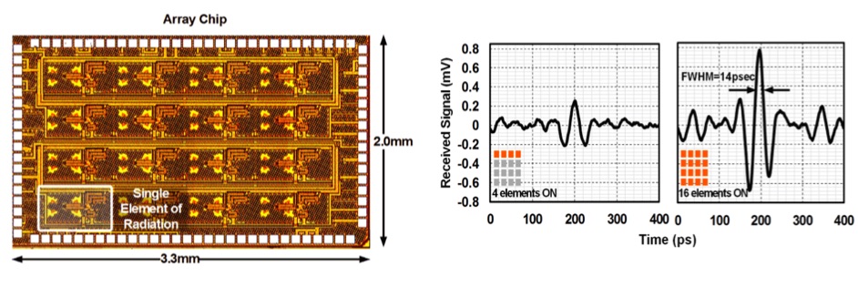
In this paper, a fully-integrated 4×4 digital-to- impulse radiating array with a programmable delay at each element is reported. Coherent spatial combining from 16 elements is successfully demonstrated. The combined signal from 16 elements achieves a jitter of 230fsec, a pulse width of 14psec, and an EIRP of 17dBm. Each array element is equipped with an 8-bit digitally-programmable delay that provides a step resolution of 200fsec and a dynamic range of 20psec. The chip is implemented in a 65nm bulk CMOS process.
Sub-picosecond Wireless Synchronization Based on a Millimeter-Wave Impulse Receiver with an On-chip Antenna in 0.13µm SiGe BiCMOS, "
in IEEE MTT-S Int. Microwave Symposium, May. 2016.
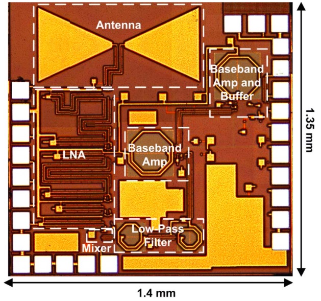
This paper presents a wireless synchronization receiver using sub-8psec pulses. A novel self-mixing technique is introduced to detect low-power picosecond impulses and extract the repetition rate with a low timing jitter. The chip is fabricated in a 0.13μm SiGe BiCMOS process and achieves a time transfer accuracy of 376fsec. The receiver, which is integrated with a broadband on-chip antenna, successfully detects a picosecond pulse train with a 3.1GHz repetition rate and generates an output locked to this rate with a phase noise of -89 dBc/Hz at 100 Hz frequency offset. The chip consumes 146 mW from a 2.5V supply and occupies an area of 1.89mm2.
A Wirelessly Powered Injection-Locked Oscillator with On-Chip Antennas in 180nm SOI CMOS, "
in IEEE MTT-S Int. Microwave Symposium, May. 2016.
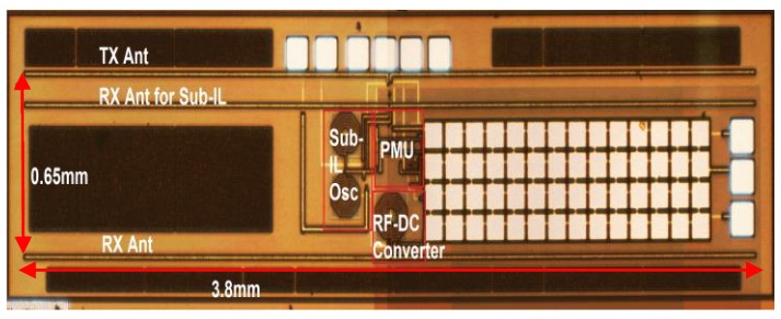
This paper presents a battery-less mm-sized wirelessly powered injection-locked oscillator with on-chip antennas in 180nm SOI CMOS. The chip harvests electromagnetic radiation from a continuous-wave source in the X-band using an on-chip antenna. In addition, the chip is equipped with a broadband injection-locking oscillator that locks to the frequency of the input and produces a synchronized signal at the half frequency of the input. The new signal is then radiated back using an on-chip dipole antenna. This architecture resolves the conventional self-interference issue in RFID sensors by separating the received and transmitted frequencies. In addition, the locking mechanism improves the phase-noise of the on-chip oscillator to -93dBc/Hz at 100Hz offset.
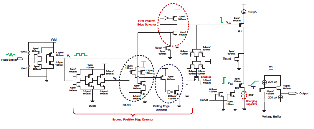
"An Ultra-Wideband Impulse Receiver for sub-100fsec Time-Transfer and sub-30µm Localization, "
in IEEE Radio and Wireless Symp. Dig. Papers, Jan. 2016.(Finalist for Best Paper Award)
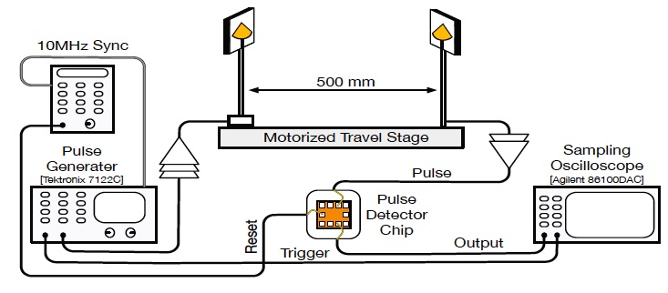
This paper presents an ultra-wideband impulse receiver capable of detecting sub-200psec pulses. The chip detects a specific zero-crossing of an incoming pulse and mitigates the undesired effects of ringing. The time detection sensitivity of the chip is limited by the jitter of the incoming pulse rather than the pulse width. A mean RMS jitter of 94fsec is recorded, which translates to the localization accuracy of sub-30µm. The chip is fabricated in IBM 130nm SiGe BiCMOS process technology.
"A 0.2-2.6GHz Instantaneous Frequency-to-Voltage Converter in 90nm CMOS, "
in IEEE Radio and Wireless Symp. Dig. Papers, Jan. 2016.
This paper presents a novel architecture for detecting the frequency of sinusoidal or square-wave signals with a short settling time. The architecture is based on detecting consecutive rising edges of the input signal and is able to generate a dc voltage proportional to the signal frequency in a time as short as only one input cycle. Measurements show that it can detect signals with frequencies up to 2.6 GHz. The chip is fabricated in a 90nm CMOS process. The total die area is 0.132 mm2 and consumes 6.5 mW from a 1-V power supply.
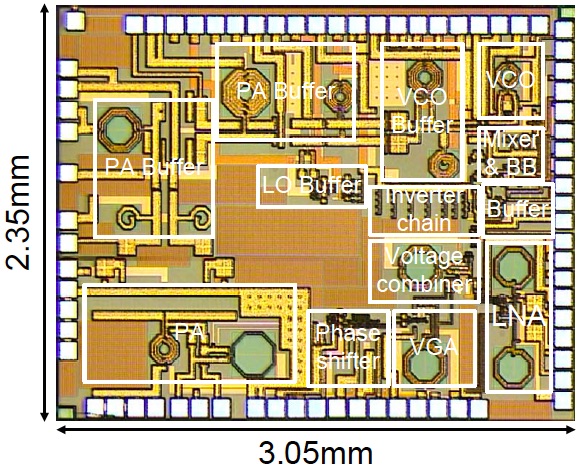
"Wireless Synchronization of mm-wave Arrays in 65nm CMOS,"
in IEEE CICC Symp. Dig. Papers, Sept. 2015.
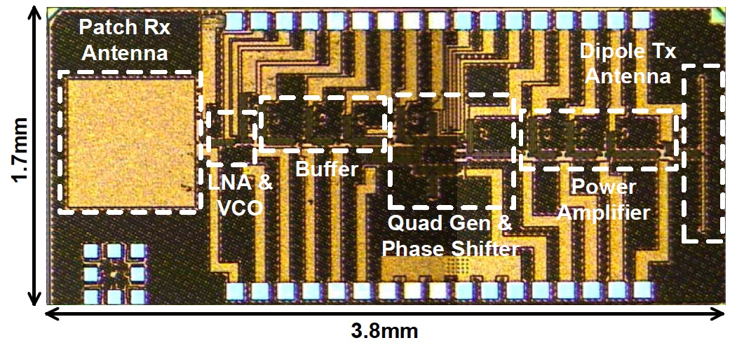
This paper presents the first wireless
synchronization of a mm-wave array, eliminating the need
for connecting wires between the array elements. Wireless
injection locking is successfully demonstrated and a 3dB
bandwidth of 400Hz at a carrier frequency of 50GHz is
achieved (frequency stability of 8ppb). The chip includes two
on-chip antennas, a power amplifier, a phase-shifter, buffer
amplifiers, and a VCO. The chip is fabricated in a 65nm
CMOS process and occupies an area of 1.7mm x 3.8mm.
A Single-Chip Electron Paramagnetic Resonance Transceiver in 0.13µm SiGe BiCMOS
in IEEE Transactions on Microwave Theory and Techniques, Oct. 2015.
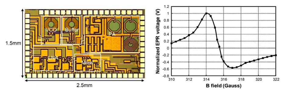
We report the first absorption-based single-chip transceiver for electron paramagnetic resonance (EPR) spectroscopy in silicon. The chip is implemented in a 0.13µm SiGe BiCMOS process technology. The transmitter generates and delivers a continuous-wave microwave signal with a frequency range from 895 to 979 MHz and the receiver adopts a direct-conversion architecture. Based on the single-chip transceiver and a printed-circuit-board-based planar resonator, an EPR spectrometer is assembled and tested. The spectrometer successfully measures the EPR response from samples including 2,2-Diphenyl-1-Picrylhydrazyl powder, Fe3O4 nanoparticles, and Fe2O3 nanoparticles.
"A 4.6-5.35GHz Transceiver with 38dB On-Chip Self-Interference Cancelation at 10kHz Offset Frequency,"
in IEEE RFIC Symp. Dig. Papers, May 2015. (Finalist for Best Paper Award))
A 4.6-5.35GHz transceiver with active selfinterference
cancelation is reported. The active cancelation
circuit cancels up to 38dB of TX leakage at 10kHz offset
from the RX signal. It increases the interference P1dB from
-25dBm to -8dBm, and RX gain by 15dB. When the
transceiver is utilized in a magnetic resonance spectroscopy
system, the SNR improves by 15dB. Furthermore, in addition
to the traditional method of B0-sweep, for the first time, the
method of frequency-sweep is demonstrated.
"A 30GHz Impulse Radiator with On-Chip Antennas for High-Resolution 3D Imaging,"
in IEEE Radio and Wireless Symp. Dig. Papers, Jan. 2015. (Best Paper Award)
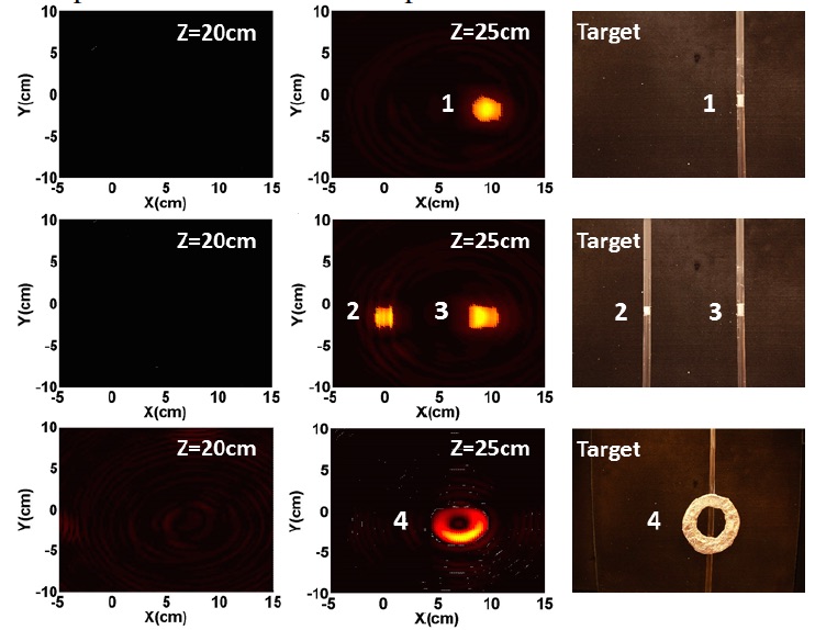
This paper reports a 30-GHz impulse radiator
utilizing an injection-locked asymmetric cross-coupled
voltage-control-oscillator (VCO) with on-chip bow-tie
antennas. The impulse radiator converts a digital trigger
signal to a radiated impulse with a variable pulse-width
down to 60psec with peak EIRP of 15.2dBm without using
any lens. Coherent spatial pulse combining is demonstrated
by using two widely spaced radiators. A timing jitter of the
216fsec for the combined signal is measured. The impulse
radiator has the capability of producing 3D images with
depth resolution of 33um at 25cm of target distance in the
air. The chip is implemented in a 0.13um SiGe BiCMOS
process technology. The total die area is 2.85mm2 with
maximum power consumption of 106mW.
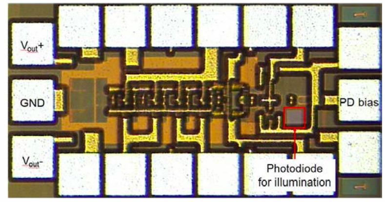
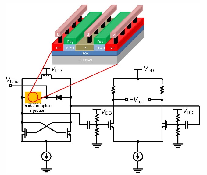
"A Free-space Optically-Locked VCO with Picosecond Timing Jitter in 0.18µm CMOS,"
in IEEE Photonics Technology Letters , vol. 26, no. 12, pp. 1180-1183, Jun. 2014.
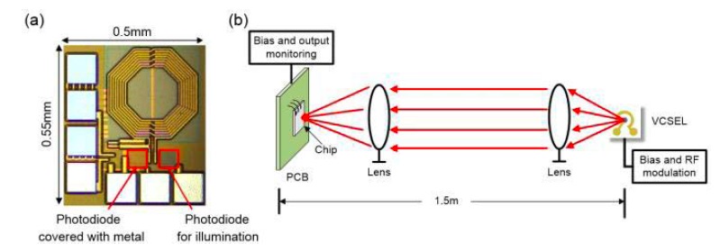
In this letter, we present a novel receiver for time
transfer that achieves picosecond accuracy through a line-of-sight
link. The receiver is based on a fully integrated optically locked
voltage controlled oscillator (OL-VCO) and is implemented in
a commercial CMOS process. The design of optical photodiodes
integrated with the OL-VCO is explained in detail. It is
demonstrated that in the locked mode, the OL-VCO can be
synchronized with a 1.3-GHz RF source through a free-space
optical link. The free-space synchronization improves the phase
noise of the OL-VCO by 25 dB at 100-Hz offset frequency.
It is shown that a time transfer accuracy of picosecond can be
achieved over a distance of 1.5 m. This represents more than two
orders of magnitude improvement compared with the prior art.
"A 9-psec Differential Lens-Less Digital-to-Impulse Radiator with 150-fs-Resolution Delay Line in Silicon,"
in IEEE RFIC Symp. Dig. Papers, Jun. 2014.
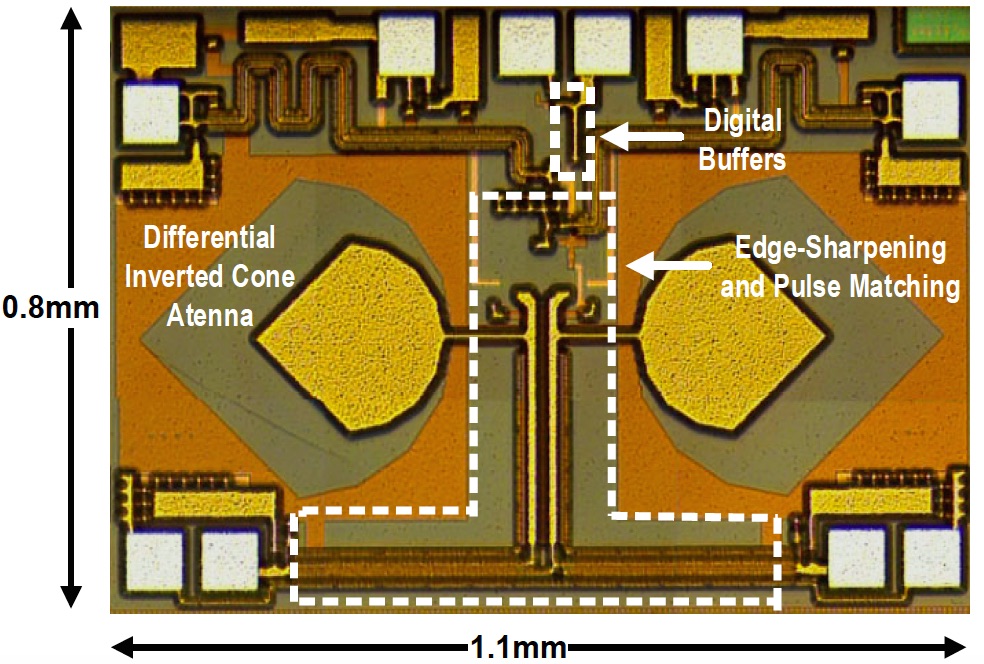
In this paper, a lens-less digital-to-impulse
radiator is implemented that radiates impulses with EIRP of
10dBm and a record pulse-width of shorter than 9psec using
an on-chip differential inverted cone antenna. It is shown that
the starting time of the radiated impulses can be locked to the
edge of the input trigger with high timing accuracy. A digitally
programmable delay line is implemented and used at the input
of the radiator. The delay line has a resolution step of 150fs
and a dynamic range of 400ps. It is shown that by
programming the delay line, the starting time of the radiated
impulses in the air can be controlled.
"A 2.5Gb/s 0.38mm2 Optical Receiver with Integrated Photodiodes in 0.18µm CMOS SOI,"
in IEEE MTT-S Int. Microwave Symposium, Jun. 2014.
In this work, we report an optical receiver with integrated photodiodes operating at 850nm wavelength. The receiver achieves a data-rate of 2.5Gb/s without using any equalizer. To minimize the area, no inductors are used in the design. The entire receiver occupies an area of 0.38mm2. This represents the smallest optical receiver operating at the Gb/s regime. The chip is fabricated in O.18um CMOS SOl process technology.
"A 40GS/s Track-and-Hold Amplifier with 62dB SFDR3 In 45nm CMOS SOl,"
in IEEE MTT-S Int. Microwave Symposium, Jun. 2014. (Finalist for Best Paper Award, 4th Prize)
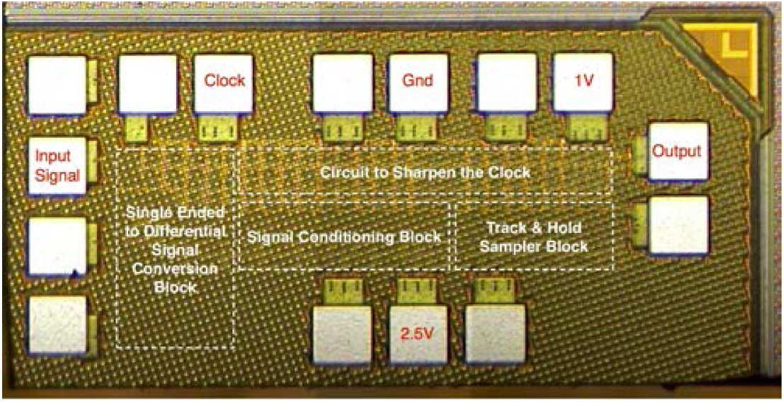
A 40GS/s Track-and-Hold amplifier with active cancellation capability is presented to mitigate the effect of leakage in transmission gate during the holding mode. A single-ended RF input signal is converted to a differential signal that feeds the active cancellation network. A record SFDR3 of 62dB with 40GS/s and SGHz input frequency is reported in 4Snm CMOS SOl. A droop voltage of 20j.lv/ns is measured. An isolation of 32dB at IGHz between the holding and tracking modes is recorded.
"An 8-psec 13dBm Peak EIRP Digital-to-Impulse Radiator with an On-chip Slot Bow-Tie Antenna in Silicon,"
in IEEE MTT-S Int. Microwave Symposium, Jun. 2014. (Best Paper Award)
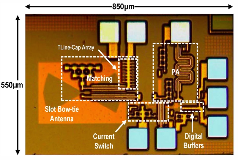
In this paper, a direct digital-to-impulse transmitter is implemented that radiates impulses with EIRP of 13dBm and a record pulse-width of shorter than 8psec. It is
shown that the starting time of the radiated impulses can be locked to the edge of the input trigger with a high timing accuracy. It is demonstrated that two widely spaced chips can generate coherent impulses in space with timing jitter of better than 270fsec. It is also shown that the frequency stability of the radiated impulses is better than 10Hz at 220GHz. The chip is fabricated in a 130nm SiGe BiCMOS process.
"Picosecond Wireless Synchronization Using an Optically Locked Voltage Controlled Oscillator (OL-VCO),"
in IEEE MTT-S Int. Microwave Symposium, Jun. 2014.
In this paper, the first fully integrated Optically Locked Voltage Controlled Oscillator (OL-VCO) is reported. The OL-VCO is locked to an RF source through a free-space optical link at 850nm. In the locked mode, the OL-VCO achieves an RMS jitter of 1.6psec with 16 averaging. It also improves the phase noise by 25dB at 100Hz offset frequency. The wireless synchronization is achieved at a distance of 1.5m, representing more than two orders of magnitude improvement compared to the prior art.
"Tumor Lysing Genetically Engineered T Cells Loaded with Multi-Modal Imaging Agents,"
in Nature Scientific Reports, 4, Article Number: 4502, pp. 1-6, Mar. 2014.
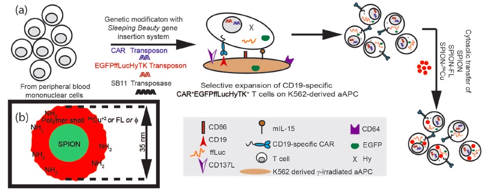
Genetically-modified T cells expressing chimeric antigen receptors (CAR) exert anti-tumor effect by
identifying tumor-associated antigen (TAA), independent of major histocompatibility complex. For
maximal efficacy and safety of adoptively transferred cells, imaging their biodistribution is critical. This will
determine if cells home to the tumor and assist in moderating cell dose. Here, T cells are modified to express
CAR. An efficient, non-toxic process with potential for cGMP compliance is developed for loading high cell
number with multi-modal (PET-MRI) contrast agents (Super Paramagnetic Iron Oxide Nanoparticles -
Copper-64; SPION-64Cu). This can now be potentially used for 64Cu-based whole-body PET to detect T cell
accumulation region with high-sensitivity, followed by SPION-based MRI of these regions for
high-resolution anatomically correlated images of T cells. CD19-specific-CAR1SPIONpos T cells effectively
target in vitro CD191 lymphoma.
"Impact of Layout on the Performance of Photodiodes in 0.18µm CMOS SOI, "
in IEEE Photonics Conference (IPC), Sept. 2013, pp. 343-346.
The impact of layout on the responsivity and bandwidth of photodiodes is studied and summarized. The photodiodes are fabricated in a 0.18um CMOS SOI process technology. The measurements are performed at wavelengths near 850nm.
"A 23.5 GHz PLL with an Adaptively Biased VCO in 32 nm SOI-CMOS,"
in IEEE Transactions on Circuits and Systems I: Regular Papers, vol. 60, no. 8, pp. 2009-2017, Aug. 2013.
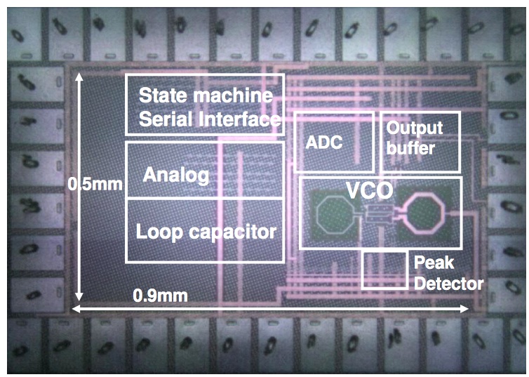
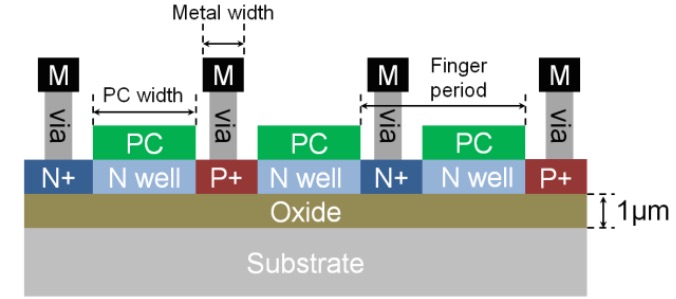
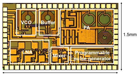
An integrated transceiver for time-domain EPR spectroscopy is implemented using a 0.13um SiGe BiCMOS technology. The system utilizes an on-chip resonator to study time domain relaxation behavior of paramagnetic samples, i.e. materials with unpaired electron spins. The single-chip EPR spectrometer consists of an EPR resonator, 22-26GHz tunable VCO, a programmable pulse generation block, RF buffer and power amplifier, a multi-stage LNA, and down-conversion mixer all in a 2mm2-size chip area.
"A Silicon-Based, Fully Integrated Pulse Electron Paramagnetic Resonance System for mm-Wave Spectroscopy, "
in IEEE MTT-S Int. Microwave Symposium, Jun. 2013.
An integrated transceiver for time-domain EPR spectroscopy is implemented using a 0.13um SiGe BiCMOS technology. The system utilizes an on-chip resonator to study time domain relaxation behavior of paramagnetic samples, i.e. materials with unpaired electron spins. The single-chip EPR spectrometer consists of an EPR resonator, 22-26GHz tunable VCO, a programmable pulse generation block, RF buffer and power amplifier, a multi-stage LNA, and down-conversion mixer all in a 2mm2-size chip area.
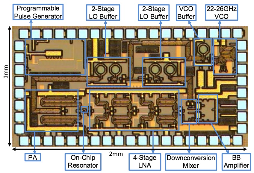
"A Single-Chip Dual-Mode CW/Pulse Electron Paramagnetic Resonance Spectrometer in 0.13µm SiGe BiCMOS, "
in IEEE MTT-S Int. Microwave Symposium, Jun. 2013.
Microwave circuitry for electron paramagnetic resonance (EPR) spectroscopy is implemented in a 0.13um SiGe BiCMOS process. The chip can operate in both continuous wave (CW) and pulse modes. The frequency is tunable from 770MHz to 970MHz, corresponding to Zeeman magnetic fields from 28mT to 35mT for a free electron. The CW-EPR absorption line of a DPPH powder sample is acquired. The chip consists of a VCO, a PA, an LNA, a down-conversion mixer, baseband amplifiers, and a pulse generation block.
"A Linearized, Low-Phase-Noise VCO-based 25-GHz PLL with Autonomic Biasing, "
in IEEE J. Solid-State Circuits, vol. 48, no. 5, pp. 1138-1150, May 2013.
This paper describes a new approach to low-phase-noise
LC VCO design based on transconductance linearization
of the active devices. A prototype 25 GHz VCO based on this linearization
approach is integrated in a dual-path PLL and achieves
superior performance compared to the state of the art. The design
is implemented in 32 nm SOI CMOS technology and achieves a
phase noise of 130 dBc/Hz at a 10 MHz offset from a 22 GHz
carrier. Additionally, the paper introduces a new layout approach
for switched capacitor arrays that enables a wide tuning range
of 23%. More than 1500 measurements of the PLL across PVT
variations were taken, further validating the proposed design.
Phase noise variation across 55 dies for four different frequencies
is 0.6 dB. Also, phase noise variation across supply voltages
of 0.7-1.5 V is 2 dB and across 60 temperature variation is 3 dB.
At the 25 GHz center frequency, the VCO is 188 dBc/Hz.
Additionally, a digitally assisted autonomic biasing technique
is implemented in the PLL to provide a phase noise and power
optimized VCO bias across frequency and process. Measurement
results indicate the efficacy of the autonomic biasing scheme.
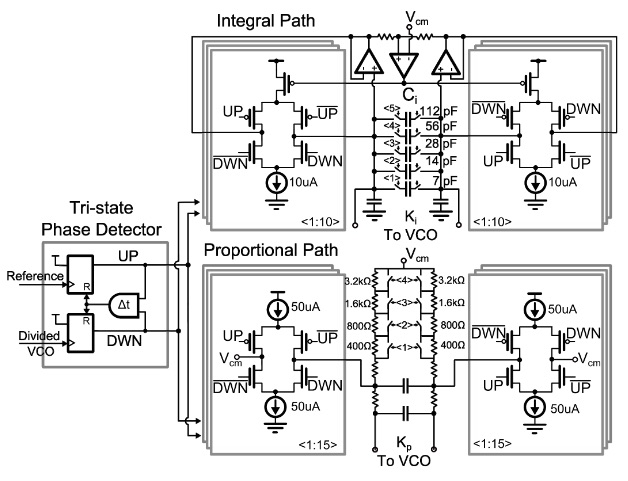
"An Integral Path Self-Calibration Scheme for a Dual-Loop PLL, "
in IEEE J. Solid-State Circuits, vol. 48, no. 4, pp. 996-1008 , Apr. 2013.
An integral-path self-calibration scheme is introduced
as part of a 20.1 GHz to 26.7 GHz low-noise PLL in 32 nm
CMOS SOI. A dual-loop architecture in combination with an
integral path measurement and correction scheme desensitizes
the loop transfer function to the VCO's small signal gain variations.
The spread of gain peaking is reduced by self-calibration
from 2.4 dB to 1 dB, when measured at 70 sites on a 300 mm
wafer. The PLL has a measured phase noise @10 MHz offset of
126.5 dBc/Hz at 20.1 GHz and 124.2 dBc/Hz at 24 GHz.
"Optical Waveguides and Photodiodes in 0.18µm CMOS SOI with No Post-processing, "
in Optical Fiber Communication (OFC) Conference, Mar. 2013
This paper demonstrates the first optical waveguide and fastest photodiode implemented in a commercial CMOS technology without performing any post-processing. The measured waveguide
loss at 1.55um is 37dB/cm and bandwidth of photodiode exceeds 9.2GHz at 850nm.
"In-plane heterostructures of graphene and hexagonal boron nitride with controlled domain sizes, "
in Nature Nanotechnology, pp. 119-124, Jan. 2013.
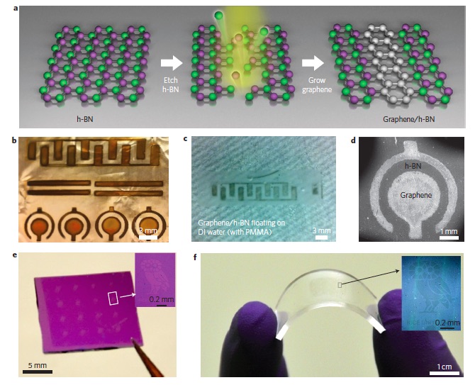
Graphene and hexagonal boron nitride (h-BN) have similar
crystal structures with a lattice constant difference of only
2%. However, graphene is a zero-bandgap semiconductor
with remarkably high carrier mobility at room temperature,
whereas an atomically thin layer of h-BN4-9 is a dielectric
with a wide bandgap of ~5.9 eV. Accordingly, if precise twodimensional
domains of graphene and h-BN can be seamlessly
stitched together, hybrid atomic layers with interesting electronic
applications could be created. Here, we show that
planar graphene/h-BN heterostructures can be formed by
growing graphene in lithographically patterned h-BN atomic
layers. Our approach can create periodic arrangements of
domains with size ranging from tens of nanometres to millimetres.
The resulting graphene/h-BN atomic layers can be
peeled off the growth substrate and transferred to various platforms
including flexible substrates.We also show that the technique
can be used to fabricate two-dimensional devices, such
as a split closed-loop resonator that works as a bandpass filter.
"An Integral Path Self-calibration Scheme for A 20.1-26.7GHz Dual-loop PLL in 32nm SOI CMOS, "
in IEEE Symposia on VLSI Technology and Circuits (VLSI), Jun. 2012, pp. 176-177.
In this paper, a bandwidth self-calibration scheme is introduced as part of a
20.1GHz to 26.7GHz, low noise PLL in 32nm CMOS SOI. A dual-loop architecture in combination with an integral path measurement and correction scheme desensitizes the loop
transfer function to the VCO's small signal gain variations. The spread of gain peaking is reduced by self-calibration from 2.4dB to 1dB, when measured at 70 sites on a 300mm wafer.
The PLL has a measured phase noise @10MHz offset of -126.5dBc/Hz at 20.1GHz.
"A 21.8-27.5GHz PLL in 32nm SOI Using Gm
Linearization to Achieve -130dBc/Hz Phase Noise at 10MHz Offset from a 22GHz Carrier,"
in IEEE RFIC Symp. Dig. Papers, Jun. 2012, pp. 75-78 .
This paper describes a new approach to low phase-noise LC VCO design based on transconductance linearization
of the active devices. A prototype 25GHz VCO based on this
approach is integrated in a dual loop PLL and achieves superior
performance compared to the state of the art. The design is
implemented in the 32nm SOI deep sub-micron CMOS technology and achieves a phase noise of
-130dBc/Hz at 10MHz offset
from a 22GHz carrier. Additionally, the paper introduces a new
layout approach for switched capacitor arrays that enables a
wide tuning range of 23%. More than 500 measurements across
PVT variations validate the proposed PLL design: phase noise
variation across 46 dies for 3 different frequencies is
smaller than 0.6dB,
across supply variation over 0.7-1.5V is 2dB and across 80C
temperature variation is 2dB. At the 25GHz center frequency,
the VCO
FOMT
is 188dBc/Hz.
Large-Scale Radiating Integrated (LSRI) Circuits
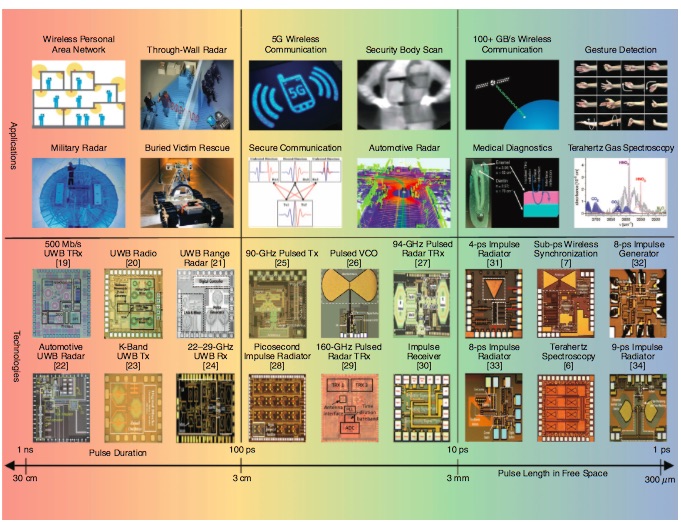
In the last few years, the dimensions of a typical silicon chip have become larger than its potential range of operating wavelengths (Figure 1). This important event has far reaching implications which are, at present, poorly understood and thus presents exciting new frontiers to explore. One of these frontiers is the field of Large-Scale Radiating Integrated (LSRI) circuits. This multidisciplinary field is a generalization/superset of several classical fields central to circuit design and encompasses applications such as high-speed wireless communication, medical imaging, bio-molecular sensing, security imaging, radar, energy-efficient near-field short distance communication, etc (Figure 2).
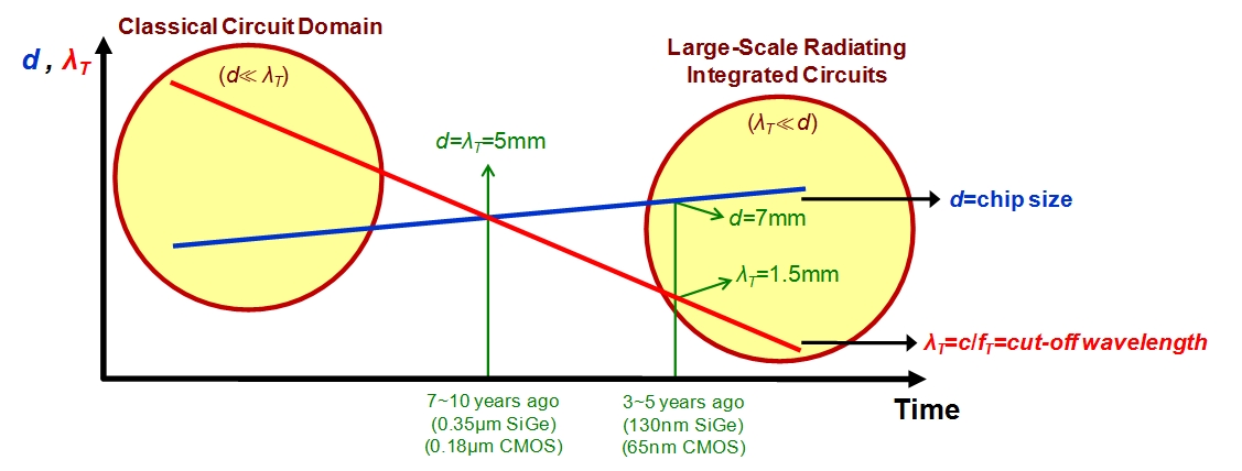
Figure 1. Chip size and cut-off wavelength
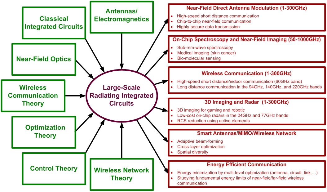
Figure 2. Large-scale radiating integrated circuits
Recognition of the birth of the field of LSRI circuits and its implications motivates reflection and rethinking of classical electronic system design research and practice. The field of LSRI circuits represents an exciting opportunity not only for hardware designers, but theorists as well. During the last several decades, an extreme and narrow focus in the individual fields of digital, mixed-mode, analog, RF/microwave, and antenna has revolutionized the semiconductor industry and significantly impacted human life. This specific form of division in electronic research fields influenced research in other areas such as wireless communication theory, network theory, control theory, and optimization theory, i.e., many problems in these theoretical fields were motivated by specific applications and their physical implementation strategies. For example, wireless communication theory discusses concepts such as base-band signal modulation and RF carrier.This originates from the efficiency limitations of small antennas. In the past, due to the low frequency contents of a base-band signal, it was not practical to connect the base-band signal directly to an antenna. Thus, the base-band signal had to be up-converted to an RF signal before being able to be sent to an antenna. Fortunately, this is no longer a limitation in today's high-speed transmitters. Today's silicon process technology makes it possible to implement chips operating in RF wavelengths that are smaller than the size of the chip itself. In these chips, information can be generated by directly modulating an antenna's boundary conditions. This concept is called Near-Field Direct Antenna Modulation (NFDAM) and introduced in [1].
The birth of LSRI circuits is an inevitable outcome of the increasing number of transistors (Moore's law) and rising transistor speed. These two important factors cause the convergence of the conventional electronic research fields (digital circuits, analog circuits, antennas) into a unified area of LSRI circuits, as illustrated in Figure 3. In order to appreciate this convergence, the complexity levels of these research fields should be discussed. The conventional electronic research fields assume different levels of abstractions that could be described by their signal-level and system-level complexities (Figure 3). For example, in a typical wireless transceiver, such as a cell phone, there are usually few antennas (low system-level complexity). The signal of these antennas could be represented with an electromagnetic wave comprised of two components (electric and magnetic fields). Each of these components is a function of time, t, and coordinates, x, y, z (high signal-level complexity). Conversely, in a digital system, the signal is usually expressed with 0's and 1's (low signal-level complexity), but the system itself could comprise several hundred million transistors (high system-level complexity). In an LSRI circuit, the signal could be a radiating electromagnetic wave (high signal-level complexity) and the system could be composed of thousands of active and passive elements (high system-level complexity).
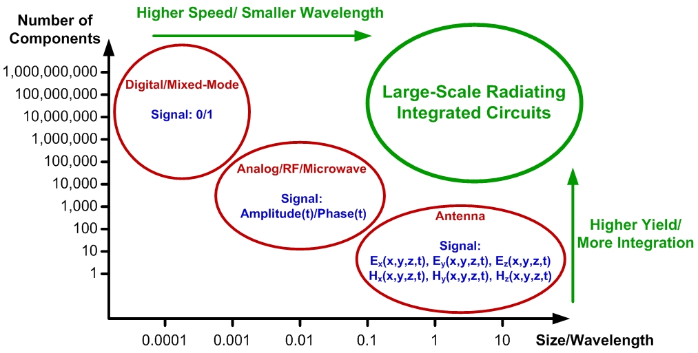
Figure 3. Signal- and system-level complexities
It should be noted that the differences in the conventional electronic research fields can also be classified by the relative size of the physical system to the operating wavelength. For an efficient antenna, the physical size is usually larger than λ/10, where λ is the wavelength in air, but the size of a digital chip could be orders of magnitude smaller than the effective wavelength (Figure 3). Traditionally, two separate approaches have been used in these research fields. The first approach originates from several decades of research on non-radiating circuits, and the second one is used primarily in studying wave-guiding and radiating structures. In the first approach, it is assumed that the physical size of a device is much smaller than the operating wavelength. This fundamental assumption reduces the complexity of Maxwell's partial differential equations by converting them into Kirchhoff's current (KCL) and voltage (KVL) laws. Although these laws are only valid for non-radiating circuits that are much smaller than the operating wavelength, they have been extremely useful in designing large-scale non-radiating integrated circuits. In the second approach, numerical techniques are used to directly solve Maxwell's partial differential equations, but, due to the practical limits on available computational power, the complexity of these systems is very limited.
The separation in these research approaches made sense in the past, as the speed of transistors was not high enough to justify the integration of radiating elements. Due to the low operating frequency of transistors, the chip size was always much smaller than the wavelength. Hence, it was not possible to make efficient on-chip radiators. Today's silicon process technology allows us to implement silicon chips that are comparable to or even larger than the operating wavelength. For example, in a typical 130nm SiGe process, which has been accessible to universities for the last 3-5 years, the length of a typical chip could be as large as 6-7mm. This process technology provides transistors with maximum cut-off frequency (fT) of close to 200GHz. In this process, the minimum cut-off wavelength of the transistor, λT, defined as the speed of light divided by the transistor's cut-off frequency, is 1.5mm. A transistor with a cut-off wavelength of λT can amplify a signal with a frequency of less than fT =c/λT, where c is the speed of light in vacuum.
As illustrated in Figure 1, we have passed the crossover
point where the chip size, d, and cut-off wavelength of
the transistors, λT, met each other. This means that the
unparalleled integration level of today's standard
silicon technology can be exploited to implement
thousands of active and passive radiating elements on a
single chip, with an unprecedented level of adaptivity
and reconfigureability. Finally, we are witnessing the
birth of large-scale radiating integrated circuits
(Figures 1, 2, 3).
It is important to realize that the fundamental laws of
classic circuit theory, i.e., Kirchhoff's current (KCL)
and voltage (KVL) laws, cannot be used to study LSRI
circuits, because radiation effects cannot be ignored
anymore. Since there are no analytical solutions for
most of these radiation problems, numerical techniques
are commonly used. During the last decade, in order to
facilitate the design process of radiating structures,
generic optimization techniques, such as genetic
algorithms, have been widely employed. Because these
genetic algorithms are usually slow and only find
locally optimum solutions, they are not very effective
when dealing with problems where hundreds or thousands of
optimization variables are involved. In a recent paper
[2], for the first time, a convex optimization method
was introduced that is capable of finding globally
optimum solutions for a broad class of large-scale
radiating integrated circuits. In order to fully utilize
the potential of today's silicon technology and speed up
the progress of designing these radiating circuits,
efficient tools for design and synthesis should be
developed.
I believe the study of large-scale radiating integrated circuits will have a significant impact in several areas:
1) LSRI can greatly influence research on millimeter-wave and sub-millimeter-wave systems, which has been rapidly advancing in the last few years. This field encompasses applications such as high-speed wireless communication, radar, medical imaging, and security imaging, as well as spectroscopy and biomedical sensing. Fortunately, some of these applications, such as high-speed wireless communication in the 60GHz unlicensed band, as well as radar and security imaging in the 94GHz band, have received significant attention from government and industry, as evidenced by the recent allocation of funding to these areas. This has provided a great opportunity for funding academic research in the millimeter and sub-millimeter wavelength regimes.
2) The study of LSRI circuits presents a new opportunity for designing novel communication systems with unique properties such as the transmitter architectures based on the concept of Near-Field Direct Antenna Modulation (NFDAM). Unlike the conventional systems, NFDAM transmitters generate information after the antenna by modulating the antenna's boundary conditions. This allows them to transmit direction-dependent information using a single antenna. This property can be exploited to increase the security of wireless communication by preventing receivers in undesired directions from capturing the correctly modulated signal, i.e., undesired receivers will receive scrambled information. This also allows a single transmitter to increase the effective data rate by simultaneously sending independent information in different directions.
3) Traditional high data-rate links are reaching the point where the loss of copper-based connections is becoming a limiting factor. Many research groups have already started looking into replacements such as inductive and capacitive proximity communication as well as optical links [3]. The study of large-scale radiating integrated circuits will help us to explore the fundamental limits of high-speed near-field wireless links, and may provide insight into superior solutions to this problem.
4) The study of large-scale radiating integrated circuits, and developing design tools for these circuits, will help us explore complex near-field wave propagation problems. The nature of many of these problems is analogous to the problems that are studied in the growing area of near-field optics. The results of such a study could be used to improve the design of optical structures, such as nano-antennas [4].
5) Historically, control theory has had a significant impact in the field of circuit design, such as the analysis and synthesis of passive linear systems in the frequency domain. Since the seminal work [5], there has been remarkable progress in characterizing passive (dissipative) systems using the concept of positive real functions. The application of control theory in circuit and communication areas evidently goes beyond the passivity concept. Indeed, the emerging optimization tools developed by control theorists, such as linear matrix inequalities (LMIs) [6] and sum-of-squares (SOS) [7], have been successfully applied to a number of fundamental problems in these fields. The study of large-scale radiating integrated circuits motivates many new challenging problems in control theory and optimization. For instance, in reference [2], a convex optimization method is introduced for finding the global optimum solution for a broad class of passive large-scale radiating circuits. Another interesting problem would be the stability analysis of large-scale radiating integrated circuits, where thousands of passive and active radiating elements are highly coupled to each-other. Some of these problems cannot be modeled using finite dimensional networks and require a stability study of Maxwell equations in the presence of continuous active boundary conditions.
6) Recently, there has been a growing interest in
studying smart antennas for increasing the effective
data rate in MIMO systems and wireless networks. The
concept of near-field direct antenna modulation
introduced in [1] is an ultimate smart antenna system
where signal modulation and beam steering are done
concurrently at the antenna level. A study of
fundamental limitations of data transmission in the
near-field direct antenna modulation systems opens many
collaboration opportunities among researchers in
communication theory, wireless network theory,
optimization theory, circuit design, and
electromagnetics. This can potentially affect the
research being done on the capacity limits of MIMO
systems, as well as that being done on developing the
scheduling and beam-steering algorithms in wireless
networks.
Self-Healing Mixed-Signal Integrated Circuits
As transistors become smaller, their performance becomes more vulnerable to process variation and mismatch. This can significantly lower the yield of a system in high volume production. Fortunately, the increasing number of available active and passive devices can be used to alleviate the problem by implementing self-healing circuits (Figure 4). These circuits, which contain sensing and controlling blocks, could constantly measure the performance of the system and autonomously vary some predefined knobs to minimize the performance degradation. As an example, in a transmitter, RF and DC power detectors, temperature sensors, and diode peak detectors can be used to measure a transmitter's gain, input and output power, linearity, and efficiency. Having these parameters, an on-chip processing unit can be used to control on-chip actuators, hence minimizing performance degradation due to process, mismatch, temperature, aging, and environment variation. These actuators could be variable impedances, variable transmission lines, gain control circuitry, etc.
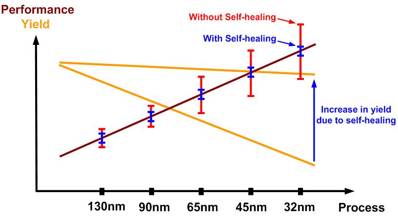
Figure 4. Self-healing increases the yield in high-volume production
References:
[1] A. Babakhani, D. B. Rutledge, and A. Hajimiri, "Transmitter Architectures Based On Near-Field Direct Antenna Modulation (NFDAM)," in IEEE J. Solid-State Circuits, vol. 43, no. 12, pp. 2674-2692, Dec. 2008.
[2] J. Lavaei, A. Babakhani, and A. Hajimiri, and J.C. Doyle, "Solving Large-Scale Linear Circuit Problems Via Convex Optimization," in IEEE Conference on Decision and Control, Dec. 2009.
[3] D. A. B. Miller, "Device Requirements for Optical Interconnects to Silicon Chips," Proc. IEEE, pp. 1166 - 1185, 2009.
[4] P. J. Schuck, et. al., "Improving The Mismatch Between Light And Nanoscale Objects With Gold Bowtie Nanoantennas," Phys. Rev. Lett. 94, 017402, 2005.
[5] O. Brune, "Synthesis Of A Finite Two Terminal Network Whose Driving Point Impedance Is A Prescribed Function Of Frequency," Journal of Mathematics and Physics, vol. 10, pp. 191-236, 1931.
[6] S. Boyd, L. E. Ghaoui, E. Feron, and V. Balakrishnan, "Linear Matrix Inequalities In System And Control Theory," SIAM, 1994.
[7] P. A. Parrilo, "Structured Semidefinite Programs And Semialgebraic Geometry Methods In Robustness And Optimization," Ph.D. dissertation, California Institute of Technology, 2000.